JAJSSV1B December   2017  – January 2024 FPC202

PRODUCTION DATA  

  1.   1
  2. 特長
  3. アプリケーション
  4. 概要
  5. Device Comparison Table
  6. Pin Configuration and Functions
  7. Specifications
    1. 6.1 Absolute Maximum Ratings
    2. 6.2 ESD Ratings
    3. 6.3 Recommended Operating Conditions
    4. 6.4 Thermal Information
    5. 6.5 Electrical Characteristics
    6. 6.6 Timing Requirements
    7. 6.7 Switching Characteristics
    8. 6.8 Typical Characteristics
  8. Detailed Description
    1. 7.1 Overview
    2. 7.2 Functional Block Diagram
    3. 7.3 Feature Description
      1. 7.3.1  Host-Side Control Interface
      2. 7.3.2  LED Control
        1. 7.3.2.1 Configurations with up to eight LEDs per port
      3. 7.3.3  Low-Speed Output Signal Control
      4. 7.3.4  Low-Speed Input Status and Interrupt Generation
      5. 7.3.5  Downstream (Port-Side) I2C Master
      6. 7.3.6  Data Pre-Fetch From Modules
      7. 7.3.7  Scheduled Write
      8. 7.3.8  Protocol Timeouts
      9. 7.3.9  General-Purpose Inputs/Outputs
      10. 7.3.10 Hot-Plug Support
    4. 7.4 Device Functional Modes
      1. 7.4.1 I2C Host-Side Control Interface
      2. 7.4.2 SPI Host-Side Control Interface
        1. 7.4.2.1 SPI Frame Structure
        2. 7.4.2.2 SPI Read Operation
        3. 7.4.2.3 SPI Write Operation
    5. 7.5 Programming
  9. Application and Implementation
    1. 8.1 Application Information
    2. 8.2 Typical Application
      1. 8.2.1 SFP/QSFP Port Management
        1. 8.2.1.1 Design Requirements
        2. 8.2.1.2 Detailed Design Procedure
        3. 8.2.1.3 Application Curves
    3. 8.3 Power Supply Recommendations
      1. 8.3.1 Power Supply Sequencing
    4. 8.4 Layout
      1. 8.4.1 Layout Guidelines
      2. 8.4.2 Layout Example
  10. Device and Documentation Support
    1. 9.1 Documentation Support
      1. 9.1.1 Related Documentation
    2. 9.2 ドキュメントの更新通知を受け取る方法
    3. 9.3 サポート・リソース
    4. 9.4 Trademarks
    5. 9.5 静電気放電に関する注意事項
    6. 9.6 用語集
  11. 10Revision History
  12. 11Mechanical, Packaging, and Orderable Information

パッケージ・オプション

メカニカル・データ(パッケージ|ピン)
サーマルパッド・メカニカル・データ
発注情報

Application Curves

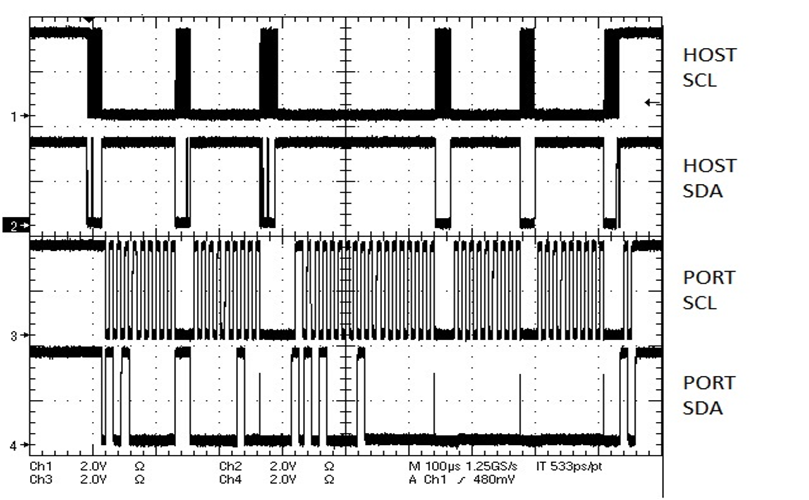
GUID-51A05F43-11A2-4B97-92C8-742AF18F208D-low.png
Host-Side I2C: 400 kHz
Port I2C: 100 kHz
Approximate time to read three bytes: 820 µs
Figure 8-4 Downstream Read – Three Bytes Outside of Pre-Fetched Range
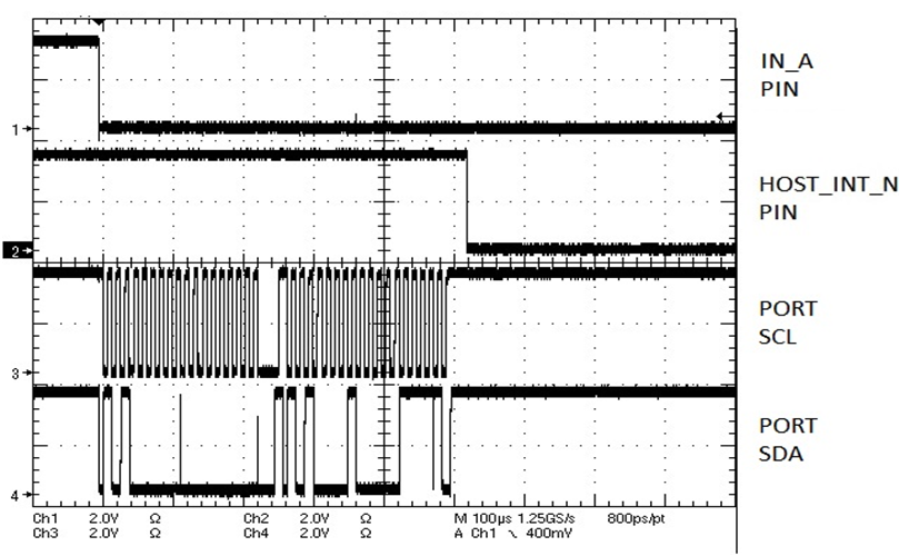
GUID-2B70D192-DBA9-48FF-986A-5266F2C96F27-low.png
Figure 8-6 Interrupt-Driven Pre-Fetch
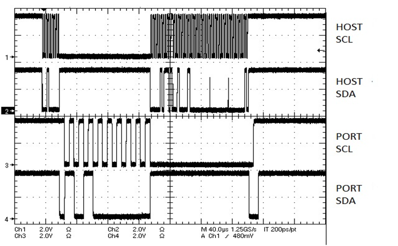
GUID-C02C3DDF-FCE3-4844-BE04-A8810D0227C0-low.png
Host-Side I2C: 400 kHz
Port I2C: 100 kHz
Approximate time to read three bytes: 280 µs
Figure 8-5 Downstream Read – Three Bytes in the Pre-Fetched Range
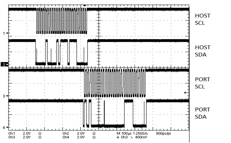
GUID-A8136EF7-71BF-401A-9E50-4A4850CD5EF0-low.png
Figure 8-7 Scheduled Write Operation