JAJSR59F March 2008 – August 2023 ISO1176
PRODUCTION DATA
- 1
- 1 特長
- 2 アプリケーション
- 3 概要
- 4 Revision History
- 5 Pin Configuration and Functions
-
6 Specifications
- 6.1 Absolute Maximum Ratings
- 6.2 ESD Ratings
- 6.3 Recommended Operating Conditions
- 6.4 Thermal Information
- 6.5 Power Ratings
- 6.6 Insulation Specifications
- 6.7 Safety-Related Certifications
- 6.8 Safety Limiting Values
- 6.9 Electrical Characteristics: Driver
- 6.10 Electrical Characteristics: Receiver
- 6.11 Supply Current
- 6.12 Electrical Characteristics: ISODE-Pin
- 6.13 Switching Characteristics: Driver
- 6.14 Switching Characteristics: Receiver
- 6.15 Insulation Characteristics Curves
- 6.16 Typical Characteristics
- 7 Parameter Measurement Information
- 8 Detailed Description
- 9 Application and Implementation
- 10Power Supply Recommendations
- 11Layout
- 12Device and Documentation Support
- 13Mechanical, Packaging, and Orderable Information
パッケージ・オプション
メカニカル・データ(パッケージ|ピン)
- DW|16
サーマルパッド・メカニカル・データ
- DW|16
発注情報
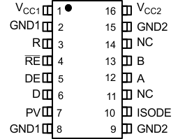
5 Pin Configuration and Functions
 Figure 5-1 DW Package
16-Pin SOIC
Top View
Table 5-1 Pin Functions
| PIN | I/O | DESCRIPTION | |
|---|---|---|---|
| NAME | NO. | ||
| A | 12 | I/O | Noninverting bus output |
| B | 13 | I/O | Inverting bus output |
| D | 6 | I | Driver input |
| DE | 5 | I | Driver logic-high enable |
| GND1 | 2, 8 | — | Logic-side ground; internally connected |
| GND2 | 9, 15 | — | Bus-side ground; internally connected |
| ISODE | 10 | — | Bus-side driver enable output |
| NC | 11, 14 | — | Not connected internally; may be left floating |
| PV | 7 | I | ISO1176 chip enable, logic
high applied immediately after power up for device operation. A logic low 3-states all outputs. |
| R | 3 | O | Receiver output |
| RE | 4 | I | Receiver logic-low enable |
| VCC1 | 1 | — | Logic side power supply |
| VCC2 | 16 | — | Bus side power supply |