JAJSDE5 June 2017
PRODUCTION DATA.
- 1 特長
- 2 アプリケーション
- 3 概要
- 4 改訂履歴
- 5 Pin Configuration and Functions
- 6 Specifications
- 7 Detailed Description
- 8 Application and Implementation
- 9 Power Supply Recommendations
- 10Layout
- 11デバイスおよびドキュメントのサポート
- 12メカニカル、パッケージ、および注文情報
7 Detailed Description
7.1 Overview
The LF442-MIL dual low power operational amplifiers provide many of the same AC characteristics as the industry standard LM1458 while greatly improving the DC characteristics of the LM1458. The amplifiers have the same bandwidth, slew rate, and gain (10 kΩ load) as the LM1458 and only draw one tenth the supply current of the LM1458. In addition the well matched high voltage JFET input devices of the LF442-MIL reduce the input bias and offset currents by a factor of 10,000 over the LM1458. A combination of careful layout design and internal trimming ensures very low input offset voltage and voltage drift. The LF442-MIL also has a very low equivalent input noise voltage for a low power amplifier.
The LF442-MIL is pin compatible with the LM1458 allowing an immediate 10 times reduction in power drain in many applications. The LF442-MIL should be used where low power dissipation and good electrical characteristics are the major considerations.
7.2 Functional Block Diagram

7.3 Feature Description
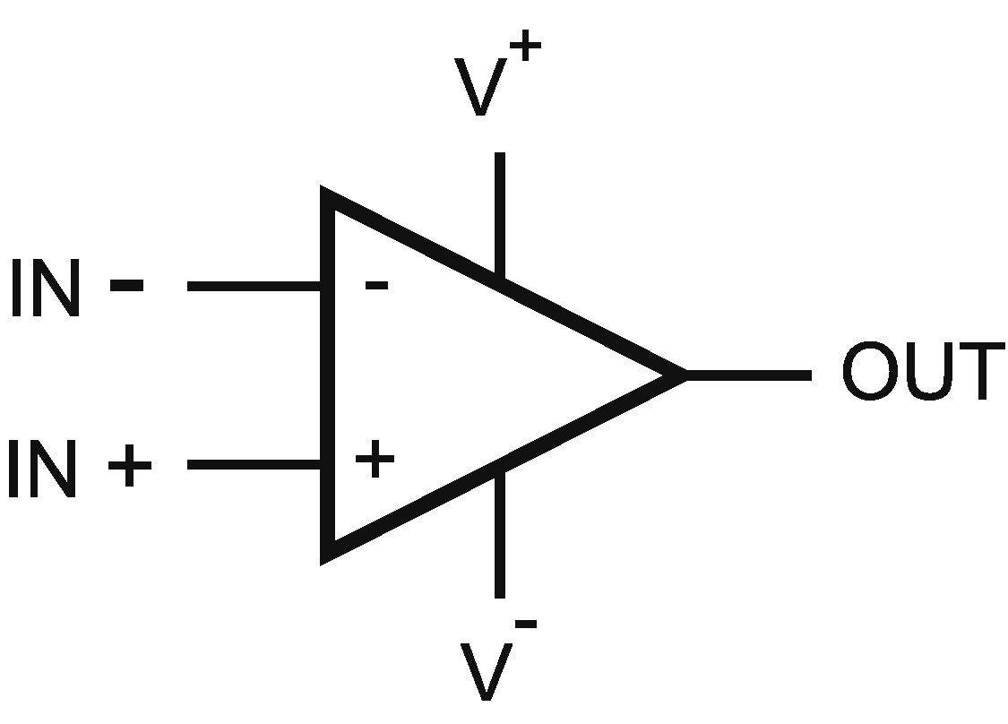
The amplifier's differential inputs consist of a non-inverting input (+IN) and an inverting input (-IN). The amplifier amplifies only the difference in voltage between the two inputs, which is called the differential input voltage. The output voltage of the op-amp VOUT is given by the equation VOUT = AOL(IN+ - IN-).
7.4 Device Functional Modes
7.4.1 Input and Output Stage
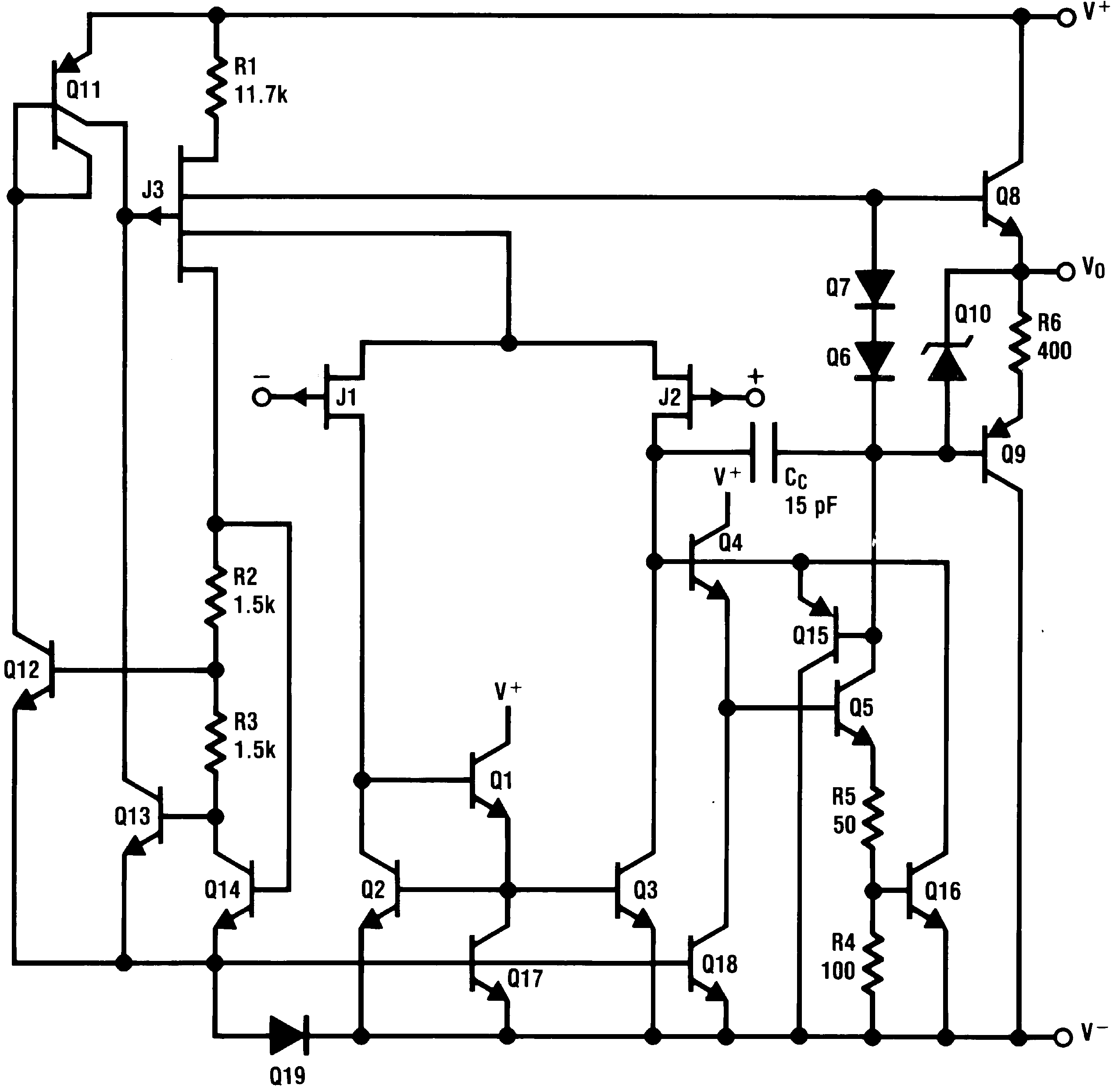
 Figure 27. 1/2 Dual LF442-MIL