JAJSB30I August 2010 – April 2018 LM25119
PRODUCTION DATA.
- 1 特長
- 2 アプリケーション
- 3 概要
- 4 改訂履歴
- 5 概要(続き)
- 6 Pin Configuration and Functions
- 7 Specifications
-
8 Detailed Description
- 8.1 Overview
- 8.2 Functional Block Diagram
- 8.3
Feature Description
- 8.3.1 High Voltage Start-Up Regulator
- 8.3.2 UVLO
- 8.3.3 Enable 2
- 8.3.4 Oscillator and Sync Capability
- 8.3.5 Error Amplifiers and PWM Comparators
- 8.3.6 Ramp Generator
- 8.3.7 Current Limit
- 8.3.8 Hiccup Mode Current Limiting
- 8.3.9 Soft Start
- 8.3.10 HO and LO Output Drivers
- 8.3.11 Maximum Duty Cycle
- 8.3.12 Thermal Protection
- 8.4 Device Functional Modes
-
9 Application and Implementation
- 9.1 Application Information
- 9.2
Typical Applications
- 9.2.1
Dual-output Design Example
- 9.2.1.1 Design Requirements
- 9.2.1.2
Detailed Design Procedure
- 9.2.1.2.1 Timing Resistor
- 9.2.1.2.2 Output Inductor
- 9.2.1.2.3 Current Sense Resistor
- 9.2.1.2.4 Ramp Resistor and Ramp Capacitor
- 9.2.1.2.5 Output Capacitors
- 9.2.1.2.6 Input Capacitors
- 9.2.1.2.7 VCC Capacitor
- 9.2.1.2.8 Bootstrap Capacitor
- 9.2.1.2.9 Soft Start Capacitor
- 9.2.1.2.10 Restart Capacitor
- 9.2.1.2.11 Output Voltage Divider
- 9.2.1.2.12 UVLO Divider
- 9.2.1.2.13 MOSFET Selection
- 9.2.1.2.14 MOSFET Snubber
- 9.2.1.2.15 Error Amplifier Compensation
- 9.2.1.3 Application Curves
- 9.2.2 Two-Phase Design Example
- 9.2.1
Dual-output Design Example
- 10Power Supply Recommendations
- 11Layout
- 12デバイスおよびドキュメントのサポート
- 13メカニカル、パッケージ、および注文情報
パッケージ・オプション
メカニカル・データ(パッケージ|ピン)
- RTV|32
サーマルパッド・メカニカル・データ
- RTV|32
発注情報
9.2.1.2.12 UVLO Divider
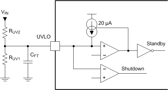
The UVLO threshold is internally set to 1.25 V at the UVLO pin. The LM25119 device is enabled when the system input voltage VIN causes the UVLO pin to exceed the threshold voltage of 1.25 V. When the UVLO pin voltage is below the threshold, the internal 20-μA current source is disabled. When the UVLO pin voltage exceeds the
1.25-V threshold, the 20-μA current source is enabled causing the UVLO pin voltage to increase, providing hysteresis. The values of RUV1 and RUV2 can be determined from Equation 34 and the example (Equation 35).


VHYS is the desired UVLO hysteresis at VIN, and VIN in the second equation is the desired UVLO release (turnon) voltage. For example, if it is desired for the LM25119 device to be enabled when VIN reaches 5.6 V, and the desired hysteresis is 1.05 V, then RUV2 must be set to 52.5 kΩ and RUV1 must be set to 15.1 kΩ. For this application, RUV2 was selected to be 52.3 kΩ and RUV1was selected to be 15 kΩ. The LM25119 device can be remotely shutdown by taking the UVLO pin below 0.4 V with an external open-collector or open-drain device. The outputs and the VCC regulator are disabled in shutdown mode. Capacitor CFT provides filtering for the divider. A value of 100 pF was chosen for CFT. The voltage at the UVLO pin must never exceed 15 V when using the external set-point divider. It may be necessary to clamp the UVLO pin at high input voltages.
 Figure 17. UVLO Configuration