JAJSJK6D October   2007  – August 2020 LM5067

PRODUCTION DATA  

  1. 特長
  2. アプリケーション
  3. 概要
  4. Revision History
  5. Device Comparison
  6. Pin Configuration and Functions
    1.     Pin Functions
  7. Specifications
    1. 7.1 Absolute Maximum Ratings
    2. 7.2 ESD Ratings
    3. 7.3 Recommended Operating Conditions
    4. 7.4 Thermal Information
    5. 7.5 Electrical Characteristics
    6. 7.6 Switching Characteristics
    7. 7.7 Typical Characteristics
  8. Detailed Description
    1. 8.1 Overview
    2. 8.2 Functional Block Diagram
    3. 8.3 Feature Description
      1. 8.3.1 Power Up Sequence
      2. 8.3.2 Gate Control
      3. 8.3.3 Current Limit
      4. 8.3.4 Circuit Breaker
      5. 8.3.5 Power Limit
      6. 8.3.6 Fault Timer and Restart
      7. 8.3.7 Undervoltage Lock-Out (UVLO)
      8. 8.3.8 Overvoltage Lock-Out (OVLO)
      9. 8.3.9 Power Good Pin
    4. 8.4 Device Functional Modes
      1. 8.4.1 Shutdown / Enable Control
  9. Application and Implementation
    1. 9.1 Application Information
    2. 9.2 Typical Application
      1. 9.2.1 Design Requirements
      2. 9.2.2 Detailed Design Procedure
        1. 9.2.2.1  RIN, CIN
        2. 9.2.2.2  Current Limit, RS
        3. 9.2.2.3  Power Limit Threshold
        4. 9.2.2.4  Turn-On Time
          1. 9.2.2.4.1 Turn-on With Current Limit Only
          2. 9.2.2.4.2 Turn-on With Power Limit and Current Limit
        5. 9.2.2.5  MOSFET Selection
        6. 9.2.2.6  Timer Capacitor, CT
          1. 9.2.2.6.1 Insertion Delay
          2. 9.2.2.6.2 Fault Timeout Period
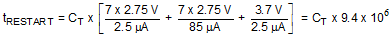
          3. 9.2.2.6.3 Restart Timing
        7. 9.2.2.7  UVLO, OVLO
          1. 9.2.2.7.1 Option A:
          2. 9.2.2.7.2 Option B:
          3. 9.2.2.7.3 Option C:
          4. 9.2.2.7.4 Option D:
        8. 9.2.2.8  Thermal Considerations
        9. 9.2.2.9  System Considerations
          1. 9.2.2.9.1 System Considerations During Surge Events
        10. 9.2.2.10 Power Good Pin
      3. 9.2.3 Application Curves
  10. 10Power Supply Recommendations
    1. 10.1 Operating Voltage
  11. 11Layout
    1. 11.1 Layout Guidelines
    2. 11.2 Layout Example
  12. 12Device and Documentation Support
    1. 12.1 Trademarks
    2. 12.2 静電気放電に関する注意事項
    3. 12.3 Glossary
  13. 13Mechanical, Packaging, and Orderable Information

パッケージ・オプション

メカニカル・データ(パッケージ|ピン)
サーマルパッド・メカニカル・データ
発注情報
Restart Timing

If the LM5067-2 is in use, after the Fault Timeout Period described above, CT is discharged by the 2.5 µA current sink to 1.25 V. The TIMER pin then cycles through seven additional charge/discharge cycles between 1.25 V and 4 V as shown in Figure 8-5. The restart time ends when the TIMER pin voltage reaches 0.3 V during the final high-to-low ramp. The restart time, after the Fault Timeout Period, is equal to:

Equation 9. GUID-5FC68073-8AC0-4679-8A28-AEA9D8C7B61A-low.gif

For example, if CT = 0.33 µF, tRESTART = 3.1 seconds. At the end of the restart time, Q1 is switched on. If the fault is still present, the fault timeout and restart sequence repeats. The on-time duty cycle of Q1 is approximately 0.5% in this mode.