JAJSJK6D October   2007  – August 2020 LM5067

PRODUCTION DATA  

  1. 特長
  2. アプリケーション
  3. 概要
  4. Revision History
  5. Device Comparison
  6. Pin Configuration and Functions
    1.     Pin Functions
  7. Specifications
    1. 7.1 Absolute Maximum Ratings
    2. 7.2 ESD Ratings
    3. 7.3 Recommended Operating Conditions
    4. 7.4 Thermal Information
    5. 7.5 Electrical Characteristics
    6. 7.6 Switching Characteristics
    7. 7.7 Typical Characteristics
  8. Detailed Description
    1. 8.1 Overview
    2. 8.2 Functional Block Diagram
    3. 8.3 Feature Description
      1. 8.3.1 Power Up Sequence
      2. 8.3.2 Gate Control
      3. 8.3.3 Current Limit
      4. 8.3.4 Circuit Breaker
      5. 8.3.5 Power Limit
      6. 8.3.6 Fault Timer and Restart
      7. 8.3.7 Undervoltage Lock-Out (UVLO)
      8. 8.3.8 Overvoltage Lock-Out (OVLO)
      9. 8.3.9 Power Good Pin
    4. 8.4 Device Functional Modes
      1. 8.4.1 Shutdown / Enable Control
  9. Application and Implementation
    1. 9.1 Application Information
    2. 9.2 Typical Application
      1. 9.2.1 Design Requirements
      2. 9.2.2 Detailed Design Procedure
        1. 9.2.2.1  RIN, CIN
        2. 9.2.2.2  Current Limit, RS
        3. 9.2.2.3  Power Limit Threshold
        4. 9.2.2.4  Turn-On Time
          1. 9.2.2.4.1 Turn-on With Current Limit Only
          2. 9.2.2.4.2 Turn-on With Power Limit and Current Limit
        5. 9.2.2.5  MOSFET Selection
        6. 9.2.2.6  Timer Capacitor, CT
          1. 9.2.2.6.1 Insertion Delay
          2. 9.2.2.6.2 Fault Timeout Period
          3. 9.2.2.6.3 Restart Timing
        7. 9.2.2.7  UVLO, OVLO
          1. 9.2.2.7.1 Option A:
          2. 9.2.2.7.2 Option B:
          3. 9.2.2.7.3 Option C:
          4. 9.2.2.7.4 Option D:
        8. 9.2.2.8  Thermal Considerations
        9. 9.2.2.9  System Considerations
          1. 9.2.2.9.1 System Considerations During Surge Events
        10. 9.2.2.10 Power Good Pin
      3. 9.2.3 Application Curves
  10. 10Power Supply Recommendations
    1. 10.1 Operating Voltage
  11. 11Layout
    1. 11.1 Layout Guidelines
    2. 11.2 Layout Example
  12. 12Device and Documentation Support
    1. 12.1 Trademarks
    2. 12.2 静電気放電に関する注意事項
    3. 12.3 Glossary
  13. 13Mechanical, Packaging, and Orderable Information

パッケージ・オプション

メカニカル・データ(パッケージ|ピン)
サーマルパッド・メカニカル・データ
発注情報
Fault Timeout Period

- During turn-on of the output voltage, or upon detection of a fault condition where the current limit and/or power limit circuits regulate the current through Q1, CT is charged by the fault timer current source (85 µA). The Fault Timeout Period is the time required for the TIMER pin voltage to reach 4.0V above VEE, at which time Q1 is switched off. The required capacitor value for the desired Fault Timeout Period tFAULT is calculated from:

Equation 8. GUID-80E9DADC-220D-4080-9F09-114DEC2525F6-low.gif

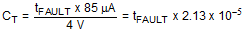
For example, if the desired Fault Timeout Period is 16 ms, CT calculates to 0.34 µF. After a fault timeout, if the LM5067-1 is in use, CT must be allowed to discharge to < 0.3 V by the 2.5 µA current sink, after which a power up sequence can be initiated by external circuitry. See Fault Timer and Restart and Latched Fault Restart Control. If the LM5067-2 is in use, after the Fault Timeout Period expires a restart sequence begins as described below (Restart Timing).

Since the LM5067 normally operates in power limit and/or current limit during a power up sequence, the Fault Timeout Period MUST be longer than the time required for the output voltage to reach its final value. See Turn-On Time.