JAJSI48C March   2017  – October 2019 LMH1228

PRODUCTION DATA.  

  1. 特長
  2. アプリケーション
  3. 概要
    1.     ブロック概略図
  4. 改訂履歴
  5. Pin Configuration and Functions
    1.     Pin Functions
  6. Specifications
    1. 6.1 Absolute Maximum Ratings
    2. 6.2 ESD Ratings
    3. 6.3 Recommended Operating Conditions
    4. 6.4 Thermal Information
    5. 6.5 Electrical Characteristics
    6. 6.6 Recommended SMBus Interface Timing Specifications
    7. 6.7 Serial Parallel Interface (SPI) Timing Specifications
    8. 6.8 Typical Characteristics
  7. Detailed Description
    1. 7.1 Overview
    2. 7.2 Functional Block Diagram
    3. 7.3 Feature Description
      1. 7.3.1 4-Level Input Pins and Thresholds
      2. 7.3.2 OUT0_SEL and SDI_OUT2_SEL Control
      3. 7.3.3 Input Signal Detect
      4. 7.3.4 Continuous Time Linear Equalizer (CTLE)
      5. 7.3.5 Clock and Data (CDR) Recovery
      6. 7.3.6 Internal Eye Opening Monitor (EOM)
      7. 7.3.7 Output Function Control
      8. 7.3.8 Output Driver Control
        1. 7.3.8.1 Line-Side Output Cable Driver (SDI_OUT1+, SDI_OUT2+)
          1. 7.3.8.1.1 Output Amplitude (VOD)
          2. 7.3.8.1.2 Output Pre-Emphasis
          3. 7.3.8.1.3 Output Slew Rate
          4. 7.3.8.1.4 Output Polarity Inversion
        2. 7.3.8.2 Host-Side 100-Ω Output Driver (OUT0±)
      9. 7.3.9 Status Indicators and Interrupts
        1. 7.3.9.1 LOCK_N (Lock Indicator)
        2. 7.3.9.2 SD_N (Signal Detect)
        3. 7.3.9.3 INT_N (Interrupt)
    4. 7.4 Device Functional Modes
      1. 7.4.1 System Management Bus (SMBus) Mode
        1. 7.4.1.1 SMBus Read and Write Transaction
          1. 7.4.1.1.1 SMBus Write Operation Format
          2. 7.4.1.1.2 SMBus Read Operation Format
      2. 7.4.2 Serial Peripheral Interface (SPI) Mode
        1. 7.4.2.1 SPI Read and Write Transactions
        2. 7.4.2.2 SPI Write Transaction Format
        3. 7.4.2.3 SPI Read Transaction Format
        4. 7.4.2.4 SPI Daisy Chain
    5. 7.5 Register Maps
  8. Application and Implementation
    1. 8.1 Application Information
      1. 8.1.1 SMPTE Requirements and Specifications
      2. 8.1.2 Low-Power Optimization
      3. 8.1.3 Optimized Loop Bandwidth Settings for Arria 10 FPGA Applications
    2. 8.2 Typical Applications
      1. 8.2.1 Dual Cable Driver
        1. 8.2.1.1 Design Requirements
        2. 8.2.1.2 Detailed Design Procedure
        3. 8.2.1.3 Application Curves
      2. 8.2.2 Distribution Amplifier
        1. 8.2.2.1 Design Requirements
        2. 8.2.2.2 Detailed Design Procedure
        3. 8.2.2.3 Application Curves
  9. Power Supply Recommendations
  10. 10Layout
    1. 10.1 Layout Guidelines
      1. 10.1.1 Board Stack-Up and Ground References
      2. 10.1.2 High-Speed PCB Trace Routing and Coupling
        1. 10.1.2.1 SDI_OUT1± and SDI_OUT2±:
        2. 10.1.2.2 IN0± and OUT0±:
      3. 10.1.3 Anti-Pads
      4. 10.1.4 BNC Connector Layout and Routing
      5. 10.1.5 Power Supply and Ground Connections
      6. 10.1.6 Footprint Recommendations
    2. 10.2 Layout Example
  11. 11デバイスおよびドキュメントのサポート
    1. 11.1 ドキュメントのサポート
      1. 11.1.1 関連資料
    2. 11.2 ドキュメントの更新通知を受け取る方法
    3. 11.3 サポート・リソース
    4. 11.4 商標
    5. 11.5 静電気放電に関する注意事項
    6. 11.6 輸出管理に関する注意事項
    7. 11.7 Glossary
  12. 12メカニカル、パッケージ、および注文情報
    1. 12.1 Package Option Addendum
      1. 12.1.1 Packaging Information
      2. 12.1.2 Tape and Reel Information

パッケージ・オプション

メカニカル・データ(パッケージ|ピン)
サーマルパッド・メカニカル・データ
発注情報

SMBus Read and Write Transaction

SMBus is a two-wire serial interface through which various system component chips can communicate with the master. Slave devices are identified by having a unique device address. The two-wire serial interface consists of SCL and SDA signals. SCL is a clock output from the master to all of the slave devices on the bus. SDA is a bidirectional data signal between the master and slave devices. The LMH1228 SMBus SCL and SDA signals are open-drain and require external pullup resistors.

Start and Stop:

The master generates Start and Stop patterns at the beginning and end of each transaction.

  • Start: High-to-low transition (falling edge) of SDA while SCL is high.
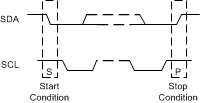
  • Start: High-to-low transition (falling edge) of SDA while SCL is high.

LMH1228 start_stop_conditions_snls515.gifFigure 12. Start and Stop Conditions

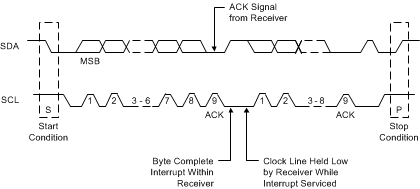
The master generates nine clock pulses for each byte transfer. The 9th clock pulse constitutes the ACK cycle. The transmitter releases SDA to allow the receiver to send the ACK signal. An ACK is recorded when the device pulls SDA low, while a NACK is recorded if the line remains high.
LMH1228 acknowledge_ack_snls515.gifFigure 13. Acknowledge (ACK)