JAJSEV5E February 2018 – July 2020 LMR23625
PRODUCTION DATA
- 1 特長
- 2 アプリケーション
- 3 概要
- 4 Revision History
- 5 Pin Configuration and Functions
- 6 Specifications
-
7 Detailed Description
- 7.1 Overview
- 7.2 Functional Block Diagram
- 7.3
Feature Description
- 7.3.1 Fixed-Frequency Peak-Current-Mode Control
- 7.3.2 Adjustable Output Voltage
- 7.3.3 Enable/Sync
- 7.3.4 VCC, UVLO
- 7.3.5 Minimum ON-time, Minimum OFF-time and Frequency Foldback at Drop-out Conditions
- 7.3.6 Internal Compensation and CFF
- 7.3.7 Bootstrap Voltage (BOOT)
- 7.3.8 Overcurrent and Short-Circuit Protection
- 7.3.9 Thermal Shutdown
- 7.4 Device Functional Modes
-
8 Application and Implementation
- 8.1 Application Information
- 8.2
Typical Applications
- 8.2.1 Design Requirements
- 8.2.2
Detailed Design Procedure
- 8.2.2.1 Custom Design With WEBENCH® Tools
- 8.2.2.2 Output Voltage Setpoint
- 8.2.2.3 Switching Frequency
- 8.2.2.4 Inductor Selection
- 8.2.2.5 Output Capacitor Selection
- 8.2.2.6 Feed-forward Capacitor
- 8.2.2.7 Input Capacitor Selection
- 8.2.2.8 Bootstrap Capacitor Selection
- 8.2.2.9 VCC Capacitor Selection
- 8.2.2.10 Undervoltage Lockout Set-Point
- 8.2.3 Application Curves
- 9 Power Supply Recommendations
- 10Layout
- 11Device and Documentation Support
- 12Mechanical, Packaging, and Orderable Information
パッケージ・オプション
デバイスごとのパッケージ図は、PDF版データシートをご参照ください。
メカニカル・データ(パッケージ|ピン)
- DDA|8
- DRR|12
サーマルパッド・メカニカル・データ
発注情報
8.2 Typical Applications
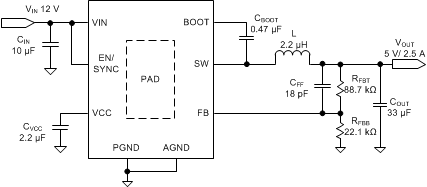
The LMR23625 only requires a few external components to convert from a wide voltage range supply to a fixed output voltage. Figure 8-1 shows a basic schematic.
 Figure 8-1 Application Circuit
The external components must fulfill the needs of the application, but also the stability criteria of the device control loop. Table 8-1 can be used to simplify the output filter component selection.
Table 8-1 L, COUT and CFF Typical Values
| fSW (kHz) | VOUT (V) | L (µH) (1) | COUT (µF) (2) | CFF (pF) | RFBT (kΩ)(3)(4) |
|---|---|---|---|---|---|
| 2100 | 3.3 | 2.2 | 47 | 33 | 51 |
| 2100 | 5 | 2.2 | 33 | 18 | 88.7 |
(1) Inductance value is calculated based on VIN = 20 V.
(2) All the COUT values are after derating. Add more when using ceramic capacitors.
(3) RFBT = 0 Ω for VOUT = 1 V. RFBB = 22.1 kΩ for all other VOUT setting.
(4) For designs with RFBT other than recommended value, adjust CFF so that (CFF × RFBT) is unchanged and adjust RFBB so that (RFBT / RFBB) is unchanged.