JAJSHH1B May 2019 – August 2020 LP5009 , LP5012
PRODUCTION DATA
- 1 特長
- 2 アプリケーション
- 3 概要
- 4 Revision History
- 5 Description (continued)
- 6 Pin Configuration and Functions
- 7 Specifications
-
8 Detailed Description
- 8.1 Overview
- 8.2 Functional Block Diagram
- 8.3
Feature Description
- 8.3.1 PWM Control for Each Channel
- 8.3.2 LED Bank Control
- 8.3.3 Current Range Setting
- 8.3.4 Automatic Power-Save Mode
- 8.3.5 Protection Features
- 8.4 Device Functional Modes
- 8.5 Programming
- 8.6
Register Maps
- 45
- 8.6.1 DEVICE_CONFIG0 (Address = 0h) [reset = 0h]
- 8.6.2 DEVICE_CONFIG1 (Address = 1h) [reset = 3Ch]
- 8.6.3 LED_CONFIG0 (Address = 2h) [reset = 00h]
- 8.6.4 BANK_BRIGHTNESS (Address = 3h) [reset = FFh]
- 8.6.5 BANK_A_COLOR (Address = 4h) [reset = 00h]
- 8.6.6 BANK_B_COLOR (Address = 5h) [reset = 00h]
- 8.6.7 BANK_C_COLOR (Address = 6h) [reset = 00h]
- 8.6.8 LED0_BRIGHTNESS (Address = 7h) [reset = FFh]
- 8.6.9 LED1_BRIGHTNESS (Address = 8h) [reset = FFh]
- 8.6.10 LED2_BRIGHTNESS (Address = 9h) [reset = FFh]
- 8.6.11 LED3_BRIGHTNESS (Address = 0Ah) [reset = FFh]
- 8.6.12 OUT0_COLOR (Address = 0Bh) [reset = 00h]
- 8.6.13 OUT1_COLOR (Address = 0Ch) [reset = 00h]
- 8.6.14 OUT2_COLOR (Address = 0Dh) [reset = 00h]
- 8.6.15 OUT3_COLOR (Address = 0Eh) [reset = 00h]
- 8.6.16 OUT4_COLOR (Address = 0Fh) [reset = 00h]
- 8.6.17 OUT5_COLOR (Address = 10h) [reset = 00h]
- 8.6.18 OUT6_COLOR (Address = 11h) [reset = 00h]
- 8.6.19 OUT7_COLOR (Address = 12h) [reset = 00h]
- 8.6.20 OUT8_COLOR (Address = 13h) [reset = 00h]
- 8.6.21 OUT9_COLOR (Address = 14h) [reset = 00h]
- 8.6.22 OUT10_COLOR (Address = 15h) [reset = 00h]
- 8.6.23 OUT11_COLOR (Address = 16h) [reset = 00h]
- 8.6.24 RESET (Address = 17h) [reset = 00h]
- 9 Application and Implementation
- 10Power Supply Recommendations
- 11Layout
- 12Device and Documentation Support
- 13Mechanical, Packaging, and Orderable Information
パッケージ・オプション
メカニカル・データ(パッケージ|ピン)
サーマルパッド・メカニカル・データ
- RUK|20
発注情報
8.3.3 Current Range Setting
The constant-current value (ISET) of all 12 channels is set by a single external resistor, RIREF. The value of RIREF can be calculated by Equation 1.
Equation 1. 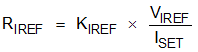
where:
- KIREF = 105
- VIREF = 0.7 V
With the IREF pin floating, the output current is close to zero. With the IREF pin shorted to GND, the LP50xx device provides internal current-limit protection, and the output-channel maximum current is limited to ILIM.
The LP50xx device supports two levels of maximum output current, IMAX.
- When VCC is in the range from 2.7 V to 5.5 V, and the Max_Current_Option (bit) = 0, IMAX = 25.5 mA.
- When VCC is in the range from 3.3 V to 5.5 V, and the Max_Current_Option (bit) = 1, IMAX = 35 mA.