JAJSLJ2J January 2011 – March 2021 OPA2836 , OPA836
PRODUCTION DATA
- 1 特長
- 2 アプリケーション
- 3 概要
- 4 Revision History
- 5 Device Comparison Table
- 6 Pin Configuration and Functions
-
7 Specifications
- 7.1 Absolute Maximum Ratings
- 7.2 ESD Ratings
- 7.3 Recommended Operating Conditions
- 7.4 Thermal Information: OPA836
- 7.5 Thermal Information: OPA2836
- 7.6 Electrical Characteristics: VS = 2.7 V
- 7.7 Electrical Characteristics: VS = 5 V
- 7.8 Typical Characteristics: VS = 2.7 V
- 7.9 Typical Characteristics: VS = 5 V
- 8 Detailed Description
-
9 Application and Implementation
- 9.1
Application Information
- 9.1.1 Noninverting Amplifier
- 9.1.2 Inverting Amplifier
- 9.1.3 Instrumentation Amplifier
- 9.1.4 Attenuators
- 9.1.5 Single-Ended-to-Differential Amplifier
- 9.1.6 Differential-to-Signal-Ended Amplifier
- 9.1.7 Differential-to-Differential Amplifier
- 9.1.8 Gain Setting With OPA836 RUN Integrated Resistors
- 9.1.9 Pulse Application With Single-Supply
- 9.1.10 ADC Driver Performance
- 9.2 Typical Applications
- 9.1
Application Information
- 10Power Supply Recommendations
- 11Layout
- 12Device and Documentation Support
- 13Mechanical, Packaging, and Orderable Information
パッケージ・オプション
メカニカル・データ(パッケージ|ピン)
サーマルパッド・メカニカル・データ
発注情報
9.2.2 Active Filters
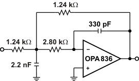
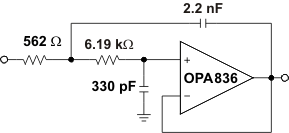
The OPA836 and OPA2836 devices are good choices for active filters. Figure 9-15 and Figure 9-16 show MFB and Sallen-Key circuits designed using the WEBENCH® Filter Designer to implement second-order low-pass Butterworth filter circuits. Figure 9-17 shows the frequency response.
Other MFB and Sallen-Key filter circuits offer similar performance. The main difference is the MFB is an inverting amplifier in the pass-band and the Sallen-Key is noninverting. The primary advantage for each is the Sallen-Key in unity gain has no resistor gain-error term, and thus no sensitivity to gain error, while the MFB has better attenuation properties beyond the bandwidth of the operational amplifier.
 Figure 9-15 MFB 100-kHz Second-Order Low-Pass Butterworth Filter Circuit
 Figure 9-16 Sallen-Key 100-kHz Second-Order Low-Pass Butterworth Filter Circuit