JAJSLJ2J January   2011  – March 2021 OPA2836 , OPA836

PRODUCTION DATA  

  1. 特長
  2. アプリケーション
  3. 概要
  4. Revision History
  5. Device Comparison Table
  6. Pin Configuration and Functions
  7. Specifications
    1. 7.1 Absolute Maximum Ratings
    2. 7.2 ESD Ratings
    3. 7.3 Recommended Operating Conditions
    4. 7.4 Thermal Information: OPA836
    5. 7.5 Thermal Information: OPA2836
    6. 7.6 Electrical Characteristics: VS = 2.7 V
    7. 7.7 Electrical Characteristics: VS = 5 V
    8. 7.8 Typical Characteristics: VS = 2.7 V
    9. 7.9 Typical Characteristics: VS = 5 V
  8. Detailed Description
    1. 8.1 Overview
    2. 8.2 Functional Block Diagrams
    3. 8.3 Feature Description
      1. 8.3.1 Input Common-Mode Voltage Range
      2. 8.3.2 Output Voltage Range
      3. 8.3.3 Power-Down Operation
      4. 8.3.4 Low-Power Applications and the Effects of Resistor Values on Bandwidth
      5. 8.3.5 Driving Capacitive Loads
    4. 8.4 Device Functional Modes
      1. 8.4.1 Split-Supply Operation (±1.25 V to ±2.75 V)
      2. 8.4.2 Single-Supply Operation (2.5 V to 5.5 V)
  9. Application and Implementation
    1. 9.1 Application Information
      1. 9.1.1  Noninverting Amplifier
      2. 9.1.2  Inverting Amplifier
      3. 9.1.3  Instrumentation Amplifier
      4. 9.1.4  Attenuators
      5. 9.1.5  Single-Ended-to-Differential Amplifier
      6. 9.1.6  Differential-to-Signal-Ended Amplifier
      7. 9.1.7  Differential-to-Differential Amplifier
      8. 9.1.8  Gain Setting With OPA836 RUN Integrated Resistors
      9. 9.1.9  Pulse Application With Single-Supply
      10. 9.1.10 ADC Driver Performance
    2. 9.2 Typical Applications
      1. 9.2.1 Audio Frequency Performance
        1. 9.2.1.1 Design Requirements
        2. 9.2.1.2 Detailed Design Procedure
        3. 9.2.1.3 Application Curves
      2. 9.2.2 Active Filters
        1. 9.2.2.1 Application Curve
  10. 10Power Supply Recommendations
  11. 11Layout
    1. 11.1 Layout Guidelines
    2. 11.2 Layout Example
  12. 12Device and Documentation Support
    1. 12.1 Device Support
      1. 12.1.1 Development Support
      2. 12.1.2 Related Documentation
    2. 12.2 Receiving Notification of Documentation Updates
    3. 12.3 サポート・リソース
    4. 12.4 静電気放電に関する注意事項
    5. 12.5 用語集
    6. 12.6 Trademarks
  13. 13Mechanical, Packaging, and Orderable Information

パッケージ・オプション

メカニカル・データ(パッケージ|ピン)
サーマルパッド・メカニカル・データ
発注情報

Typical Characteristics: VS = 5 V

at VS+ = +5 V, VS– = 0 V, VOUT = 2 VPP, RF = 0 Ω, RL = 1 kΩ, G = 1 V/V, input and output referenced to mid-supply unless otherwise noted. TA = 25°C, unless otherwise noted.
GUID-0BE00DEC-7B62-4A05-ABC9-AF1FFC694EB9-low.gif
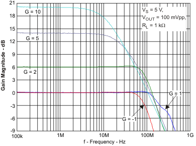
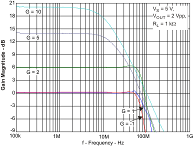
Figure 7-27 Small Signal Frequency Response
GUID-43964B5E-C8F2-4076-B278-581B3CF10316-low.gif
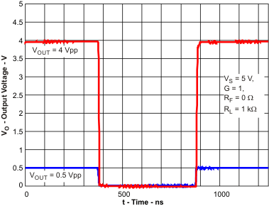
Figure 7-29 Noninverting Pulse Response
GUID-D9F37449-9830-4240-B028-EB9B41312D47-low.gif
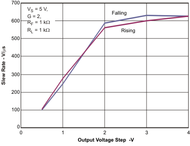
Figure 7-31 Slew Rate vs Output Voltage Step
GUID-6B48A9C8-5188-4F0C-AC82-0D3EB70464D5-low.gif
Figure 7-28 Large Signal Frequency Response
GUID-128649EE-6F20-4CDD-AF6B-3045445A8F77-low.gif
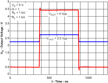
Figure 7-30 Inverting Pulse Response
GUID-FFBE45C7-596A-42D7-8D19-BFAD94F40207-low.gif
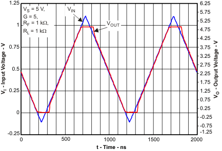
Figure 7-32 Output Overdrive Recovery

at VS+ = +5 V, VS– = 0 V, VOUT = 2 VPP, RF = 0 Ω, RL = 1 kΩ, G = 1 V/V, input and output referenced to mid-supply unless otherwise noted. TA = 25°C, unless otherwise noted.
GUID-F9266553-0347-46DF-B52A-5E6433C67F67-low.gif
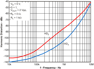
Figure 7-33 Harmonic Distortion vs Frequency
GUID-D4C4B794-7EB8-428C-B71E-5BC021484B10-low.gif
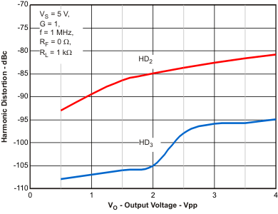
Figure 7-35 Harmonic Distortion vs Output Voltage
GUID-95E79ABE-0DBF-43FD-A5D9-E11095EFA5BA-low.gif
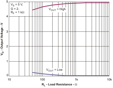
Figure 7-37 Output Voltage Swing vs Load Resistance
GUID-7677C847-301A-4940-B66D-8074E59AFFD2-low.gif
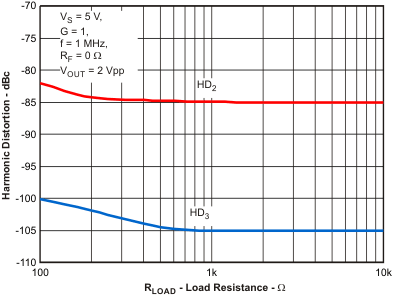
Figure 7-34 Harmonic Distortion vs Load Resistance
GUID-791110E7-C995-48A4-A166-3954BDECE6C0-low.gif
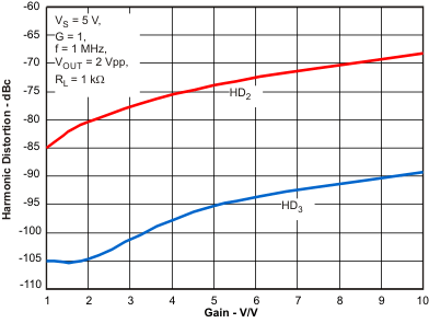
Figure 7-36 Harmonic Distortion vs Gain
GUID-D10BC426-7500-41B9-8880-840F079BA22A-low.gif
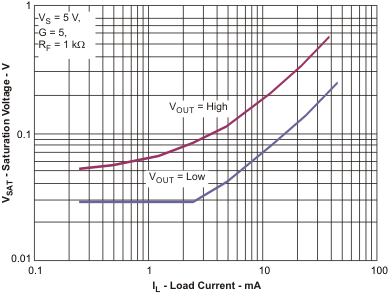
Figure 7-38 Output Saturation Voltage vs Load Current

at VS+ = +5 V, VS– = 0 V, VOUT = 2 VPP, RF = 0 Ω, RL = 1 kΩ, G = 1 V/V, input and output referenced to mid-supply unless otherwise noted. TA = 25°C, unless otherwise noted.
GUID-D3886758-6C63-4256-819E-B10AA2C56CDB-low.gif
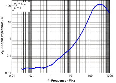
Figure 7-39 Output Impedance vs Frequency
GUID-EBD81C95-9569-478F-BD8B-5CA79BAB434D-low.png
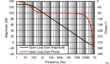
VS = 5.0 V
Figure 7-41 Open Loop Gain vs Frequency
GUID-2BDBF039-D95D-46B5-A01F-C4D7EDF9EB5C-low.gif
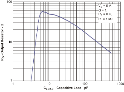
Figure 7-43 Series Output Resistor vs Capacitive Load
GUID-C39580E6-A44E-4468-A051-27321410B3D4-low.gif
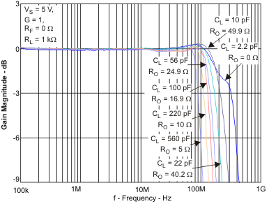
Figure 7-40 Frequency Response With Capacitive Load
GUID-DCA5F5B5-8DC7-4AD6-902B-82B3F32D5C29-low.gif
VS = 5.0 V
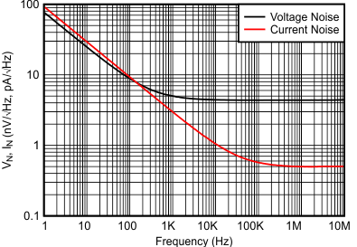
Figure 7-42 Input Referred Noise vs Frequency
GUID-F99DA3C6-AA92-49FE-82A7-73DA65348D80-low.gif
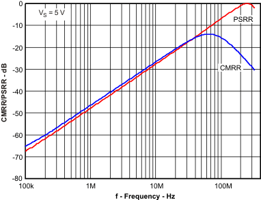
Figure 7-44 Common-Mode/Power Supply Rejection Ratios vs Frequency

at VS+ = +5 V, VS– = 0 V, VOUT = 2 VPP, RF = 0 Ω, RL = 1 kΩ, G = 1 V/V, input and output referenced to mid-supply unless otherwise noted. TA = 25°C, unless otherwise noted.
GUID-8F9A761E-1234-4540-B3A6-A31DFC1ED5A4-low.gif
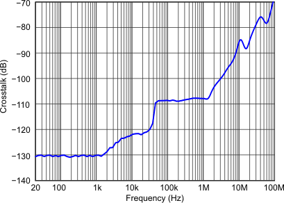
Figure 7-45 Crosstalk vs Frequency
GUID-A991FA88-4ECA-497A-A041-3CC440E46E47-low.gif
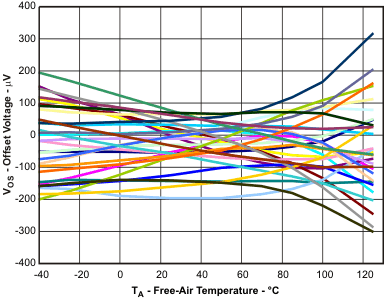
Figure 7-47 Input Offset Voltage vs Free-Air Temperature
GUID-FFDACE1C-7922-4CAB-A890-6BCE98FA3F3B-low.gif
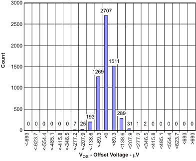
Figure 7-49 Input Offset Voltage
GUID-ED5D6E75-A38A-44EF-8885-1DA9FDD8C87F-low.gif
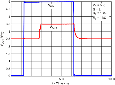
Figure 7-46 Power Down Response
GUID-3C247B0F-59B4-4ECE-845D-208AE25CFFB7-low.gif
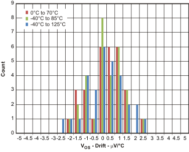
Figure 7-48 Input Offset Voltage Drift
GUID-1694AD61-E142-445D-BF3D-FAE5AC340B37-low.gif
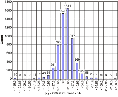
Figure 7-50 Input Offset Current

at VS+ = +5 V, VS– = 0 V, VOUT = 2 VPP, RF = 0 Ω, RL = 1 kΩ, G = 1 V/V, input and output referenced to mid-supply unless otherwise noted. TA = 25°C, unless otherwise noted.
GUID-2146285A-6420-4998-87E7-D7C53931C85B-low.gif
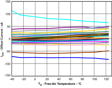
Figure 7-51 Input Offset Current vs Free-Air Temperature
GUID-17E9314D-6C7D-4D41-9CAE-9312450F8C79-low.gif
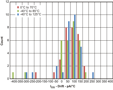
Figure 7-52 Input Offset Current Drift