SLLSEA8A January 2012 – March 2016 SN65LVCP114
PRODUCTION DATA.
- 1 Features
- 2 Applications
- 3 Description
- 4 Revision History
- 5 Description (continued)
- 6 Pin Configuration and Functions
- 7 Specifications
- 8 Parameter Measurement Information
-
9 Detailed Description
- 9.1 Overview
- 9.2 Functional Block Diagram
- 9.3 Feature Description
- 9.4 Device Functional Modes
- 9.5 Programming
- 9.6
Register Maps
- 9.6.1
SN65LVCP114 Register Mapping Information
- 9.6.1.1 Register 0x00
- 9.6.1.2 Register 0x01
- 9.6.1.3 Register 0x02
- 9.6.1.4 Register 0x03
- 9.6.1.5 Register 0x04
- 9.6.1.6 Register 0x06
- 9.6.1.7 Register 0x07
- 9.6.1.8 Register 0x08
- 9.6.1.9 Register 0x0A
- 9.6.1.10 Register 0x0B
- 9.6.1.11 Register 0x0C
- 9.6.1.12 Register 0x0D
- 9.6.1.13 Register 0x0F
- 9.6.1.14 Register 0x10
- 9.6.1.15 Register 0x11
- 9.6.1.16 Register 0x12
- 9.6.1.17 Register Descriptions
- 9.6.1
SN65LVCP114 Register Mapping Information
- 10Application and Implementation
- 11Power Supply Recommendations
- 12Layout
- 13Device and Documentation Support
- 14Mechanical, Packaging, and Orderable Information
12 Layout
12.1 Layout Guidelines
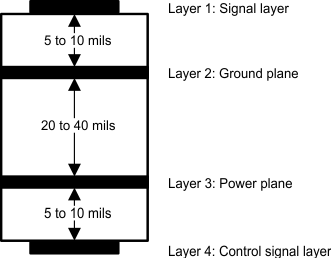
TI recommends using at a minimum a four-layer stack-up to accomplish a low-EMI PCB design.
- It is important to match the electrical length of these high-speed traces to minimize both inter-pair and intrapair skew.
- Placing a solid ground plane next to the high-speed signal layer establishes controlled impedance for transmission line interconnects and provides an excellent low-inductance path for the return current flow.
- Placing the power plane next to the ground plane creates additional high-frequency bypass capacitance.
- Routing the slower speed control signals on the bottom layer allows for greater flexibility as these signal links usually have margin to tolerate discontinuities such as vias.
- If an additional supply voltage plane or signal layer is needed, add a second power / ground plane system to the stack to keep it symmetrical. This makes the stack mechanically stable and prevents it from warping. Also the power and ground plane of each power system can be placed closer together, thus increasing the high frequency bypass capacitance significantly
 Figure 40. PCB Stack
12.2 Layout Example
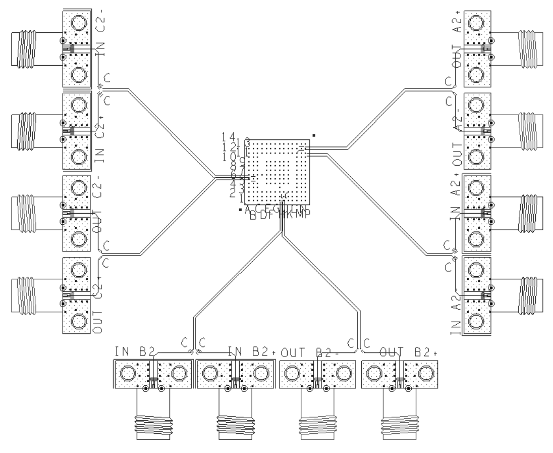
 Figure 41. Layout Example