SLLSEA8A January 2012 – March 2016 SN65LVCP114
PRODUCTION DATA.
- 1 Features
- 2 Applications
- 3 Description
- 4 Revision History
- 5 Description (continued)
- 6 Pin Configuration and Functions
- 7 Specifications
- 8 Parameter Measurement Information
-
9 Detailed Description
- 9.1 Overview
- 9.2 Functional Block Diagram
- 9.3 Feature Description
- 9.4 Device Functional Modes
- 9.5 Programming
- 9.6
Register Maps
- 9.6.1
SN65LVCP114 Register Mapping Information
- 9.6.1.1 Register 0x00
- 9.6.1.2 Register 0x01
- 9.6.1.3 Register 0x02
- 9.6.1.4 Register 0x03
- 9.6.1.5 Register 0x04
- 9.6.1.6 Register 0x06
- 9.6.1.7 Register 0x07
- 9.6.1.8 Register 0x08
- 9.6.1.9 Register 0x0A
- 9.6.1.10 Register 0x0B
- 9.6.1.11 Register 0x0C
- 9.6.1.12 Register 0x0D
- 9.6.1.13 Register 0x0F
- 9.6.1.14 Register 0x10
- 9.6.1.15 Register 0x11
- 9.6.1.16 Register 0x12
- 9.6.1.17 Register Descriptions
- 9.6.1
SN65LVCP114 Register Mapping Information
- 10Application and Implementation
- 11Power Supply Recommendations
- 12Layout
- 13Device and Documentation Support
- 14Mechanical, Packaging, and Orderable Information
7 Specifications
7.1 Absolute Maximum Ratings
over operating free-air temperature range (unless otherwise noted)(1)| MIN | MAX | UNIT | ||||
|---|---|---|---|---|---|---|
| VCC | Supply voltage range(2) | –0.3 | 4 | V | ||
| VIN,DIFF | Differential voltage between xINx_P and xINx_N | ±2.5 | V | |||
| VIN+, VIN– |
Voltage at xINx_P and xINx_N | –0.5 | VCC + 0.5 | V | ||
| VIO | Voltage on control I/O pins | –0.3 | VCC + 0.5 | V | ||
| IIN+
IIN– |
Continuous current at high-speed differential data inputs (differential) | –25 | 25 | mA | ||
| IOUT+
IOUT– |
Continuous current at high-speed differential data outputs | –25 | 25 | mA | ||
| Tstg | Storage temperature | –55 | 125 | °C | ||
(1) Stresses beyond those listed under Absolute Maximum Ratings may cause permanent damage to the device. These are stress ratings only, and functional operation of the device at these or any other conditions beyond those indicated under Recommended Operating Conditions is not implied. Exposure to absolute-maximum-rated conditions for extended periods may affect device reliability.
(2) All voltage values, except differential I/O bus voltages, are with respect to network ground terminal.
7.2 ESD Ratings
| VALUE | UNIT | |||
|---|---|---|---|---|
| V(ESD) | Electrostatic discharge | Human-body model (HBM), per ANSI/ESDA/JEDEC JS-001(1)(2) | ±2000 | V |
| Charged-device model (CDM), per JEDEC specification JESD22-C101(3)(4) | ±500 | |||
(1) JEDEC document JEP155 states that 500-V HBM allows safe manufacturing with a standard ESD control process. Manufacturing with less than 500-V HBM is possible with the necessary precautions. Pins listed as ±2000 V may actually have higher performance.
(2) Tested in accordance with JEDEC Standard 22, Test Method A114-A.
(3) JEDEC document JEP157 states that 250-V CDM allows safe manufacturing with a standard ESD control process. Manufacturing with less than 250-V CDM is possible with the necessary precautions. Pins listed as ±500 V may actually have higher performance.
(4) Tested in accordance with JEDEC Standard 22, Test Method C101.
7.3 Recommended Operating Conditions
| MIN | NOM | MAX | UNIT | ||
|---|---|---|---|---|---|
| Operating data rate, dR | 14.2 | Gbps | |||
| Supply voltage, VCC, 2.5-V nominal supply | 2.375 | 2.5 | 2.625 | V | |
| Supply voltage, VCC, 3.3-V nominal supply | 3.135 | 3.3 | 3.465 | V | |
| PSNR BG, bandgap circuitry PSNR, 10 Hz–10 GHz | 20 | dB | |||
| CONTROL INPUTS | |||||
| VIH | High-level input voltage | 0.8 × VCC | |||
| VIM | Mid-level input voltage | VCC/2 – 0.3 | VCC/2 + 0.3 | V | |
| VIL | Low- level input voltage | 0.2 × VCC | V | ||
| TC | Junction temperature(1) | –10 | 125 | °C | |
| Maximum board temperature(1) | See Table 1 | °C | |||
(1) Use of θJB and φJB are recommended for thermal calculations. For more information about traditional and new thermal metrics, see IC Package Thermal Metrics application report, SPRA953.
7.4 Thermal Information
| THERMAL METRIC(1) | SN65LVCC114 | UNIT | |
|---|---|---|---|
| ZJA (NFBGA) | |||
| 167 PINS | |||
| RθJA | Junction-to-ambient thermal resistance | 38.8 | °C/W |
| RθJC(top) | Junction-to-case (top) thermal resistance | 7.55 | °C/W |
| RθJB | Junction-to-board thermal resistance | 17.8 | °C/W |
| ψJT | Junction-to-top characterization parameter | 0.2 | °C/W |
| ψJB | Junction-to-board characterization parameter | 17.5 | °C/W |
| RθJC(bot) | Junction-to-case (bottom) thermal resistance | N/A | °C/W |
(1) For more information about traditional and new thermal metrics, see the Semiconductor and IC Package Thermal Metrics application report, SPRA953.
7.5 Electrical Characteristics (VCC 2.5 V ±5%)
over operating conditions range. All parameters are referenced to package pins (unless otherwise noted).| PARAMETER | TEST CONDITIONS | MIN | TYP | MAX | UNIT | |
|---|---|---|---|---|---|---|
| POWER CONSUMPTION | ||||||
| PDL | Device power dissipation, loopback mode | Ports A, B, and C in loopback mode with all 12 channels active. VOD = LOW | 1800 | 2300 | mW | |
| PDN | Device power dissipation, normal mode | Device configured in mux-demux mode with 8 channels active. VOD = LOW | 1400 | 1800 | mW | |
| PDOFF | Device power dissipation, lanes disabled | All 4 lanes disabled. See the I2C section for device configuration. | 50 | mW | ||
| PDSTB | Device power dissipation, standby | All 12 channels active, VOD = LOW, FAST_SW = HIGH. See the I2C section for device configuration. |
1800 | 2300 | mW | |
7.6 Electrical Characteristics (VCC 3.3 V ±5%)
over operating conditions range. All parameters are referenced to package pins (unless otherwise noted).| PARAMETER | TEST CONDITIONS | MIN | TYP | MAX | UNIT | |
|---|---|---|---|---|---|---|
| POWER CONSUMPTION | ||||||
| PDL | Device power dissipation, loopback mode | Ports A, B, and C in loopback mode with all 12 channels active. VOD = LOW | 2500 | 3150 | mW | |
| PDN | Device power dissipation, normal mode | Device configured in mux-demux mode with 8 channels active. VOD = LOW | 1800 | 2500 | mW | |
| PDOFF | Device power dissipation, lanes disabled | All 4 lanes disabled. See the I2C section for device configuration. | 50 | mW | ||
| PDSTB | Device power dissipation, standby | All 12 channels active, VOD = LOW, FAST_SW = HIGH. See I2C section for device configuration. |
2500 | 3150 | mW | |
7.7 Electrical Characteristics (VCC 3.3 V ±5%, 2.5 V ±5%)
over operating conditions range. All parameters are referenced to package pins (unless otherwise noted).| PARAMETER | TEST CONDITIONS | MIN | TYP(1) | MAX | UNIT | |
|---|---|---|---|---|---|---|
| CMOS DC SPECIFICATIONS | ||||||
| IIH | High-level input current | VIN = 0.9 × VCC | 80 | µA | ||
| IIL | Low-level input current | VIN = 0.1 × VCC | -80 | µA | ||
| CML INPUTS (AINP[3:0], AINN[3:0], BINP[3:0], BINN[3:0], CINP[3:0], CINN[3:0]) | ||||||
| rIN | Differential input resistance | INx_P to INx_N | 100 | Ω | ||
| VINPP | Input linear dynamic range | Gain = 0.5 | 1200 | mVpp | ||
| VICM | Common-mode input voltage | Internally biased | VCC – 0.3 | V | ||
| SCD11 | Input differential to common-mode conversion | 100 MHz to 7.1GHz | –25 | dB | ||
| SDD11 | Differential input return loss | 100 MHz to 7.1GHz | –10 | dB | ||
| CML OUTPUTS (AOUTP[3:0], AOUTN[3:0], BOUTP[3:0], BOUTN[3:0], COUTP[3:0], COUTN[3:0]) | ||||||
| VOD | Output linear dynamic range | RL = 100 Ω, VOD = High | 1200 | mVPP | ||
| RL = 100 Ω, VOD = Low | 600 | |||||
| VOS | Output offset voltage | RL = 100 Ω, 0 V applied at inputs | 20 | mVPP | ||
| VCM,RIP | Common-mode output ripple | K28.5 pattern at 14.2 Gbps, no interconnect loss, VOD = HIGH |
10 | 20 | mVRMS | |
| VOD,RIP | Differential path output ripple | K28.5 pattern at 14.2Gbps, no interconnect loss, VIN = 1200 mVpp. Outputs squelched. |
20 | mVPP | ||
| VOCM | Output common mode voltage | See Figure 9 | VCC – 0.35 | V | ||
| VOC(SS) | Change in steady-state common-mode output voltage between logic states | ±10 | mV | |||
| tPLH | Low-to-high propagation delay | See Figure 1 | 200 | ps | ||
| tPHL | High-to-low propagation delay | 200 | ps | |||
| tSK(O) | Inter-pair output skew (2) | All outputs terminated with 100 Ω. See Figure 3 | 50 | ps | ||
| tSK(PP) | Part-to-part skew(3) | 100 | ps | |||
| tR | Rise time | Input signal with 30-ps rise time, 20% to 80%. See Figure 2 | 31 | ps | ||
| tF | Fall time | Input signal with 30-ps fall time, 20% to 80%. See Figure 2 | 31 | ps | ||
| SDD22 | Differential output return loss | 100 MHz to 7.1 GHz | –10 | dB | ||
| SCC22 | Common-mode output return loss | 100 MHz to 7.1 GHz | –5 | dB | ||
| tSM | Multiplexer switch time | Mux to valid output (idle outputs are squelched) | 100 | ns | ||
| tSM1 | Mux to valid output (idle outputs are turned off) | 10 | μs | |||
| Chiso | Channel-to-channel isolation(4) | Frequency at 5.1625 GHz | 52.2 | dB | ||
| Frequency at 7.1 GHz | 43.5 | |||||
| OUTNOISE | Output referred noise | 10 MHz to 7.1 GHz. No other noise source present. VOD = LOW |
1500 | µVRMS | ||
| 10 MHz to 7.1 GHz. No other noise source present. VOD = HIGH |
3000 | |||||
| Vpre | Output pre-cursor pre-emphasis | Input signal with 3.75-dB pre-cursor and measured on the output signal. See Figure 4. Vpre = 20 log(V3/V2) | 5 | dB | ||
| Vpst | Output post-cursor pre-emphasis | Input signal with 12-dB post-cursor and measure on the output signal. See Figure 4. Vpst = 20 log(V1/V2) |
14 | dB | ||
| rOT | Single-ended output resistance | Single-ended on-chip terminations to VCC, outputs are AC-coupled | 50 | Ω | ||
| rOM | Output termination mismatch at 1 MHz |  |
5% | |||
| EQUALIZATION | ||||||
| EQGain | At 7.1 GHz input signal | Equalization gain, EQ = MAX | 10 | 15 | dB | |
| DJ1 | TX residual deterministic jitter at 10.3125 Gbps | Tx launch amplitude = 0.6 Vpp, EQ = 1.3 dB, VOD and GAIN are high. Test channel = 0". See Figure 11. | 0.08 | UIp-p | ||
| DJ2 | TX residual deterministic jitter at 14.2 Gbps | Tx launch amplitude = 0.6 Vpp, EQ = 1.3 dB, VOD and GAIN are high. Test channel = 0". See Figure 11. | 0.06 | UIp-p | ||
| DJ3 | RX residual deterministic jitter at 10.3125 Gbps | Tx launch amplitude = 0.6 Vpp, test channel = 12” (9-dB loss at 5 GHz), EQ = 13.9 dB, VOD and GAIN are high. See Figure 10. | 0.04 | UIp-p | ||
| DJ4 | RX residual deterministic Jitter at 14.2 Gbps | Tx launch amplitude = 0.6 Vpp, test channel = 8" (9-dB loss at 7 GHz), EQ = 13.9 dB, VOD = LOW and GAIN = HIGH. See Figure 10. | 0.08 | UIp-p | ||
(1) All typical values are at 25°C and with 2.5-V and 3.3-V supply, unless otherwise noted.
(2) tSK(O) is the magnitude of the time difference between the channels within a Port. For more information, see SN65LVCP114 Guidelines for Skew Compensation, SLLA323.
(3) tSK(PP) is the magnitude of the difference in propagation delay times between any specified terminals of two devices when both devices operate with the same supply voltages, at the same temperature, and have identical packages and test circuits.
(4) All noise sources added.
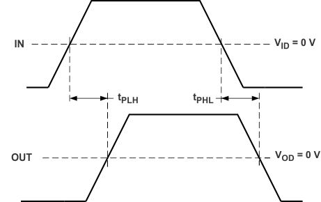 Figure 1. Propagation Delay, Input to Output
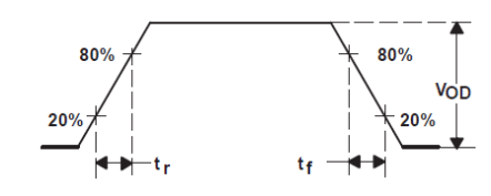 Figure 2. Output Rise and Fall Times
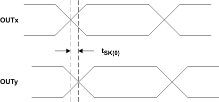 Figure 3. Output Inter-Pair Skew
![SN65LVCP114 VPRE and VPOST [The Test
Pattern is 1111111100000000 (Eight 1s, Eight 0s)] SN65LVCP114 Vpre_Vpost_llsea8.gif](/ods/images/SLLSEA8A/Vpre_Vpost_llsea8.gif) Figure 4. VPRE and VPOST [The Test Pattern is 1111111100000000 (Eight 1s, Eight 0s)]
Figure 4. VPRE and VPOST [The Test Pattern is 1111111100000000 (Eight 1s, Eight 0s)]
7.8 Typical Characteristics
Typical operating condition is at VCC = 2.5 V and TA = 25°C, no interconnect line at the output, and with default device settings (unless otherwise noted).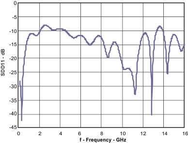 Figure 5. Differential Input Return Loss
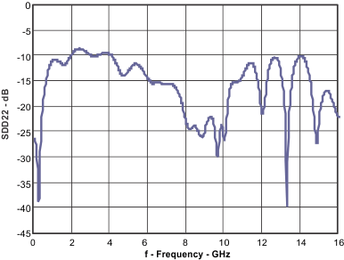 Figure 7. Differential Output Return Loss
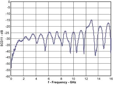 Figure 6. Differential to Common-Mode Conversion
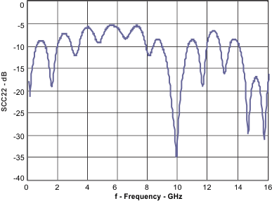 Figure 8. Common-Mode Output Return Loss