SCES551F February 2004 – March 2024 SN74AVC16T245
PRODUCTION DATA
- 1
- 1 Features
- 2 Applications
- 3 Description
- 4 Description (continued)
- 5 Pin Configuration and Functions
-
6 Specifications
- 6.1 Absolute Maximum Ratings
- 6.2 ESD Ratings
- 6.3 Recommended Operating Conditions
- 6.4 Thermal Information
- 6.5 Electrical Characteristics
- 6.6 Switching Characteristics: VCCA = 1.2 V
- 6.7 Switching Characteristics: VCCA = 1.5 V ± 0.1 V
- 6.8 Switching Characteristics: VCCA = 1.8 V ± 0.15 V
- 6.9 Switching Characteristics: VCCA = 2.5 V ± 0.2 V
- 6.10 Switching Characteristics: VCCA = 3.3 V ± 0.3 V
- 6.11 Operating Characteristics
- 6.12 Typical Characteristics
- 7 Parameter Measurement Information
- 8 Detailed Description
- 9 Application and Implementation
- 10Device and Documentation Support
- 11Revision History
- 12Mechanical, Packaging, and Orderable Information
パッケージ・オプション
メカニカル・データ(パッケージ|ピン)
サーマルパッド・メカニカル・データ
発注情報
3 Description
This 16-bit noninverting bus transceiver uses two separate configurable power-supply rails. The SN74AVC16T245 device is optimized to operate with VCCA/VCCB set at 1.4V to 3.6V. The device is operational with VCCA/VCCB as low as 1.2V. The A port is designed to track VCCA. VCCA accepts any supply voltage from 1.2V to 3.6V. The B port is designed to track VCCB. VCCB accepts any supply voltage from 1.2V to 3.6V. This allows for universal low-voltage bidirectional translation between any of the 1.2V, 1.5V, 1.8V, 2.5V, and 3.3V voltage nodes.
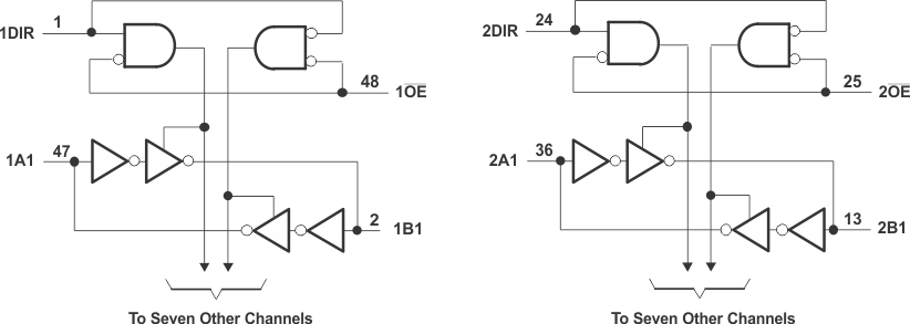
The SN74AVC16T245 device is designed for asynchronous communication between data buses. The device transmits data from the A bus to the B bus or from the B bus to the A bus, depending on the logic level at the direction-control (DIR) input. The output-enable ( OE) input can be used to disable the outputs so the buses effectively are isolated.
The SN74AVC16T245 control pins (1DIR, 2DIR, 1 OE, and 2 OE) are supplied by VCCA.
| PART NUMBER | PACKAGE(1) | BODY SIZE (NOM) |
|---|---|---|
| SN74AVC16T245 | TSSOP (48) | 12.50 mm × 6.10mm |
| TVSOP (48) | 9.70 mm × 4.40mm | |
| BGA MICROSTAR JUNIOR (56) |
7.00 mm × 4.50mm |
 Logic Diagram (Positive Logic)