JAJSJB8B June   2011  – July 2020 SN74AVC4T234

PRODUCTION DATA  

  1. 特長
  2. アプリケーション
  3. 概要
  4. Revision History
  5. Pin Configuration and Functions
  6. Specifications
    1. 6.1  Absolute Maximum Ratings
    2. 6.2  ESD Ratings
    3. 6.3  Recommended Operating Conditions
    4. 6.4  Thermal Information
    5. 6.5  Electrical Characteristics
    6. 6.6  Switching Characteristics, VCCB = 1.1 V
    7. 6.7  Switching Characteristics, VCCB = 1.4 V
    8. 6.8  Switching Characteristics, VCCB = 1.65 V
    9. 6.9  Switching Characteristics, VCCB = 2.3 V
    10. 6.10 Switching Characteristics, VCCB = 3 V
    11. 6.11 Operating Characteristics
  7. Parameter Measurement Information
    1. 7.1 Load Circuit and Voltage Waveforms
  8. Detailed Description
    1. 8.1 Overview
    2. 8.2 Functional Block Diagram
    3. 8.3 Feature Description
      1. 8.3.1 Fully Configurable Dual-Rail Design Allows Each Port to Operate Over the Full 0.9-V to 3.6-V Power-Supply Range
      2. 8.3.2 Supports High Speed Translation
      3. 8.3.3 Ioff Supports Partial-Power-Down Mode Operation
    4. 8.4 Device Functional Modes
  9. Application and Implementation
    1. 9.1 Application Information
    2. 9.2 Typical Application
      1. 9.2.1 Design Requirements
      2. 9.2.2 Detailed Design Procedure
      3. 9.2.3 Application Curves
  10. 10Power Supply Recommendations
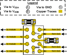
  11. 11Layout
    1. 11.1 Layout Guidelines
    2. 11.2 Layout Example
  12. 12Device and Documentation Support
    1. 12.1 サポート・リソース
    2. 12.2 Trademarks
    3. 12.3 静電気放電に関する注意事項
    4. 12.4 用語集
  13. 13Mechanical, Packaging, and Orderable Information

パッケージ・オプション

メカニカル・データ(パッケージ|ピン)
サーマルパッド・メカニカル・データ
発注情報

Layout Example

GUID-8B99FB3D-7732-468F-94DF-3D352D2D0D99-low.gif