JAJSC60E May 2016 – May 2021 THS6212
PRODUCTION DATA
- 1 特長
- 2 アプリケーション
- 3 概要
- 4 Revision History
- 5 Pin Configuration and Functions
- 6 Specifications
- 7 Detailed Description
- 8 Application and Implementation
- 9 Power Supply Recommendations
- 10Layout
- 11Device and Documentation Support
- 12Mechanical, Packaging, and Orderable Information
8.2.2.2.1 Line Driver Headroom Requirements
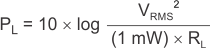
The first step in a transformer-coupled, twisted-pair driver design is to compute the peak-to-peak output voltage from the target specifications. This calculation is done using Equation 8 to Equation 11:
where
- PL = power at the load
- VRMS = voltage at the load
- RL = load impedance
These values produce the following:
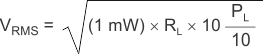

where
- VP = peak voltage at the load
- CF = crest factor

where
- VLPP = peak-to-peak voltage at the load
Consolidating Equation 8 to Equation 11 allows the required peak-to-peak voltage at the load to be expressed as a function of the crest factor, the load impedance, and the power at the load, as given by Equation 12:
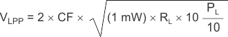
VLPP is usually computed for a nominal line impedance and can be taken as a fixed design target.
The next step in the design is to compute the individual amplifier output voltage and currents as a function of peak-to-peak voltage on the line and transformer-turns ratio.
When this turns ratio changes, the minimum allowed supply voltage also changes. The peak current in the amplifier output is given by Equation 13:
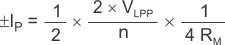
where
- VPP is as defined in Equation 12, and
- RM is as defined in Equation 7 and Figure 8-5
 Figure 8-5 Driver Peak Output Voltage
With the previous information available, a supply voltage and the turns ratio desired for the transformer can now be selected, and the headroom for the THS6212 can be calculated.
The model shown in Figure 8-6 can be described with Equation 14 and Equation 15 as:
- The available output swing:
Equation 14.

- Or as the required supply voltage:
Equation 15.

The minimum supply voltage for power and load requirements is given by Equation 15.
V1, V2, R1, and R2 are given in Table 8-1 for the ±14-V operation.
 Figure 8-6 Line Driver Headroom Model
| VS | V1 | R1 | V2 | R2 |
|---|---|---|---|---|
| ±14 V | 1 V | 0.6 Ω | 1 V | 1.2 Ω |
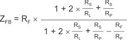
When using a synthetic output impedance circuit (see Figure 8-4), a significant drop in bandwidth occurs from the specification provided in the Electrical Characteristics tables. This apparent drop in bandwidth for the differential signal is a result of the apparent increase in the feedback transimpedance for each amplifier. This feedback transimpedance equation is given by Equation 16:
To increase the 0.1-dB flatness to the frequency of interest, adding a serial RC in parallel with the gain resistor may be needed, as shown in Figure 8-7.
 Figure 8-7 0.1-dB Flatness Compensation Circuit