JAJSGS4P November   2008  – February 2021 TMS320F28020 , TMS320F280200 , TMS320F28021 , TMS320F28022 , TMS320F28023 , TMS320F28023-Q1 , TMS320F28026 , TMS320F28026-Q1 , TMS320F28026F , TMS320F28027 , TMS320F28027-Q1 , TMS320F28027F , TMS320F28027F-Q1

PRODUCTION DATA  

  1. 特長
  2. アプリケーション
  3. 概要
  4. 機能ブロック図
  5. 改訂履歴
  6. Device Comparison
    1. 6.1 Related Products
  7. Terminal Configuration and Functions
    1. 7.1 ピン構造図
    2. 7.2 信号概要
      1. 7.2.1 信号概要
  8. 仕様
    1. 8.1  Absolute Maximum Ratings
    2. 8.2  ESD 定格 – 車載用
    3. 8.3  ESD 定格 – 民生用
    4. 8.4  推奨動作条件
    5. 8.5  消費電力の概略
      1. 8.5.1 TMS320F2802x/F280200 の消費電流 (40MHz の SYSCLKOUT)
      2. 8.5.2 TMS320F2802x の消費電流 (50MHz)
      3. 8.5.3 TMS320F2802x の消費電流 (60MHz の SYSCLKOUT)
      4. 8.5.4 Reducing Current Consumption
      5. 8.5.5 消費電流グラフ (VREG 有効)
    6. 8.6  電気的特性
    7. 8.7  熱抵抗特性
      1. 8.7.1 PT パッケージ
      2. 8.7.2 DA パッケージ
    8. 8.8  熱設計の検討事項
    9. 8.9  MCU との JTAG デバッグ・プローブ接続 (信号バッファリングなし)
    10. 8.10 パラメータ情報
      1. 8.10.1 タイミング・パラメータの記号
      2. 8.10.2 タイミング・パラメータに関する一般的な注意事項
    11. 8.11 テスト負荷回路
    12. 8.12 電源シーケンス
      1. 8.12.1 リセット (XRS) のタイミング要件
      2. 8.12.2 リセット (XRS) のスイッチング特性
    13. 8.13 クロック仕様
      1. 8.13.1 デバイス・クロック表
        1. 8.13.1.1 2802x のクロックの一覧表 (40MHz デバイス)
        2. 8.13.1.2 2802x のクロックの一覧表 (50MHz デバイス)
        3. 8.13.1.3 2802x のクロックの一覧表 (60MHz デバイス)
        4. 8.13.1.4 デバイス・クロック要件 / 特性
        5. 8.13.1.5 内部のゼロ・ピン発振器 (INTOSC1、INTOSC2) の特性
      2. 8.13.2 クロックの要件と特性
        1. 8.13.2.1 XCLKIN のタイミング要件 – PLL 有効
        2. 8.13.2.2 XCLKIN のタイミング要件 – PLL 無効
        3. 8.13.2.3 XCLKOUT のスイッチング特性 (PLL バイパスまたは有効)
    14. 8.14 フラッシュのタイミング
      1. 8.14.1 T 温度仕様品のフラッシュ / OTP 耐久性
      2. 8.14.2 S 温度仕様品のフラッシュ / OTP 耐久性
      3. 8.14.3 Q 温度仕様品のフラッシュ / OTP 耐久性
      4. 8.14.4 60MHz SYSCLKOUT でのフラッシュ・パラメータ
      5. 8.14.5 50MHz SYSCLKOUT でのフラッシュ・パラメータ
      6. 8.14.6 40MHz SYSCLKOUT でのフラッシュ・パラメータ
      7. 8.14.7 フラッシュ書き込み / 消去時間
      8. 8.14.8 フラッシュ / OTP のアクセス・タイミング
      9. 8.14.9 Flash Data Retention Duration
  9. 詳細説明
    1. 9.1 Overview
      1. 9.1.1  CPU
      2. 9.1.2  Memory Bus (Harvard Bus Architecture)
      3. 9.1.3  ペリフェラル・バス
      4. 9.1.4  Real-Time JTAG and Analysis
      5. 9.1.5  Flash
      6. 9.1.6  M0、M1 SARAM
      7. 9.1.7  L0 SARAM
      8. 9.1.8  Boot ROM
        1. 9.1.8.1 エミュレーション・ブート
        2. 9.1.8.2 GetMode
        3. 9.1.8.3 ブートローダが使用するペリフェラル・ピン
      9. 9.1.9  Security
      10. 9.1.10 ペリフェラル割り込み拡張 (PIE) ブロック
      11. 9.1.11 外部割り込み (XINT1~XINT3)
      12. 9.1.12 内部ゼロ・ピン発振器、発振器、PLL
      13. 9.1.13 ウォッチドッグ
      14. 9.1.14 Peripheral Clocking
      15. 9.1.15 Low-power Modes
      16. 9.1.16 ペリフェラル・フレーム 0、1、2 (PFn)
      17. 9.1.17 汎用入出力 (GPIO) マルチプレクサ (MUX)
      18. 9.1.18 32 ビット CPU タイマ (0、1、2)
      19. 9.1.19 Control Peripherals
      20. 9.1.20 シリアル・ポート・ペリフェラル
    2. 9.2 Memory Maps
    3. 9.3 Register Maps
    4. 9.4 Device Emulation Registers
    5. 9.5 VREG/BOR/POR
      1. 9.5.1 オンチップ電圧レギュレータ (VREG)
        1. 9.5.1.1 オンチップ VREG の使い方
        2. 9.5.1.2 オンチップ VREG の無効化
      2. 9.5.2 On-chip Power-On Reset (POR) and Brown-Out Reset (BOR) Circuit
    6. 9.6 システム・コントロール
      1. 9.6.1 内部ゼロ・ピン発振器
      2. 9.6.2 Crystal Oscillator Option
      3. 9.6.3 PLL-Based Clock Module
      4. 9.6.4 入力クロックの喪失 (NMI ウォッチドッグ機能)
      5. 9.6.5 CPU ウォッチドッグ・モジュール
    7. 9.7 Low-power Modes Block
    8. 9.8 Interrupts
      1. 9.8.1 External Interrupts
        1. 9.8.1.1 外部割り込みの電気的データ / タイミング
          1. 9.8.1.1.1 External Interrupt Timing Requirements
          2. 9.8.1.1.2 External Interrupt Switching Characteristics
    9. 9.9 ペリフェラル
      1. 9.9.1  Analog Block
        1. 9.9.1.1 A/D コンバータ (ADC)
          1. 9.9.1.1.1 特長
          2. 9.9.1.1.2 ADC 変換開始の電気的データ / タイミング
            1. 9.9.1.1.2.1 外部 ADC 変換開始のスイッチング特性
          3. 9.9.1.1.3 オンチップ A/D コンバータ (ADC) の電気的データ / タイミング
            1. 9.9.1.1.3.1 ADC Electrical Characteristics
            2. 9.9.1.1.3.2 ADC の電力モード
            3. 9.9.1.1.3.3 内部温度センサ
              1. 9.9.1.1.3.3.1 Temperature Sensor Coefficient
            4. 9.9.1.1.3.4 ADC パワーアップ制御ビットのタイミング
              1. 9.9.1.1.3.4.1 ADC パワーアップ遅延
            5. 9.9.1.1.3.5 ADC のシーケンシャルおよび同時タイミング
        2. 9.9.1.2 ADC MUX
        3. 9.9.1.3 コンパレータ・ブロック
          1. 9.9.1.3.1 オンチップ・コンパレータ / DAC の電気的データ / タイミング
            1. 9.9.1.3.1.1 Electrical Characteristics of the Comparator/DAC
      2. 9.9.2  詳細説明
      3. 9.9.3  Serial Peripheral Interface (SPI) Module
        1. 9.9.3.1 SPI マスタ・モードの電気的データ / タイミング
          1. 9.9.3.1.1 SPI Master Mode External Timing (Clock Phase = 0)
          2. 9.9.3.1.2 SPI Master Mode External Timing (Clock Phase = 1)
        2. 9.9.3.2 SPI スレーブ・モードの電気的データ / タイミング
          1. 9.9.3.2.1 SPI Slave Mode External Timing (Clock Phase = 0)
          2. 9.9.3.2.2 SPI Slave Mode External Timing (Clock Phase = 1)
      4. 9.9.4  Serial Communications Interface (SCI) Module
      5. 9.9.5  Inter-Integrated Circuit (I2C)
        1. 9.9.5.1 I2C の電気的データ / タイミング
          1. 9.9.5.1.1 I2C のタイミング要件
          2. 9.9.5.1.2 I2C のスイッチング特性
      6. 9.9.6  Enhanced PWM Modules (ePWM1/2/3/4)
        1. 9.9.6.1 ePWM の電気的データ / タイミング
          1. 9.9.6.1.1 ePWM Timing Requirements
          2. 9.9.6.1.2 ePWM のスイッチング特性
        2. 9.9.6.2 トリップ・ゾーン入力のタイミング
          1. 9.9.6.2.1 Trip-Zone Input Timing Requirements
      7. 9.9.7  High-Resolution PWM (HRPWM)
        1. 9.9.7.1 HRPWM の電気的データ / タイミング
          1. 9.9.7.1.1 高分解能 PWM の特性 (SYSCLKOUT = 50MHz~60MHz)
      8. 9.9.8  Enhanced Capture Module (eCAP1)
        1. 9.9.8.1 eCAP の電気的データ / タイミング
          1. 9.9.8.1.1 Enhanced Capture (eCAP) Timing Requirement
          2. 9.9.8.1.2 eCAP のスイッチング特性
      9. 9.9.9  JTAG ポート
      10. 9.9.10 General-Purpose Input/Output (GPIO) MUX
        1. 9.9.10.1 GPIO の電気的データ / タイミング
          1. 9.9.10.1.1 GPIO - 出力タイミング
            1. 9.9.10.1.1.1 汎用出力のスイッチング特性
          2. 9.9.10.1.2 GPIO - 入力タイミング
            1. 9.9.10.1.2.1 汎用入力のタイミング要件
          3. 9.9.10.1.3 入力信号のサンプリング・ウィンドウ幅
          4. 9.9.10.1.4 低消費電力モードのウェイクアップ・タイミング
            1. 9.9.10.1.4.1 IDLE Mode Timing Requirements
            2. 9.9.10.1.4.2 IDLE Mode Switching Characteristics
            3. 9.9.10.1.4.3 STANDBY モードのタイミング要件
            4. 9.9.10.1.4.4 STANDBY モードのスイッチング特性
            5. 9.9.10.1.4.5 HALT Mode Timing Requirements
            6. 9.9.10.1.4.6 HALT モードのスイッチング特性
  10. 10アプリケーション、実装、およびレイアウト
    1. 10.1 テキサス・インスツルメンツのリファレンス・デザイン
  11. 11デバイスおよびドキュメントのサポート
    1. 11.1 Device and Development Support Tool Nomenclature
    2. 11.2 Tools and Software
    3. 11.3 ドキュメントのサポート
    4. 11.4 サポート・リソース
    5. 11.5 商標
    6. 11.6 静電気放電に関する注意事項
    7. 11.7 用語集
  12. 12メカニカル、パッケージ、および注文情報
    1. 12.1 パッケージ情報

パッケージ・オプション

メカニカル・データ(パッケージ|ピン)
サーマルパッド・メカニカル・データ
発注情報

Serial Communications Interface (SCI) Module

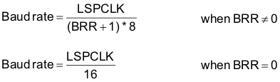
The devices include one serial communications interface (SCI) module (SCI-A). The SCI module supports digital communications between the CPU and other asynchronous peripherals that use the standard nonreturn-to-zero (NRZ) format. The SCI receiver and transmitter are double-buffered, and each has its own separate enable and interrupt bits. Both can be operated independently or simultaneously in the full-duplex mode. To ensure data integrity, the SCI checks received data for break detection, parity, overrun, and framing errors. The bit rate is programmable to over 65000 different speeds through a 16-bit baud-select register.

Features of each SCI module include:

  • Two external pins:
    • SCITXD: SCI transmit-output pin
    • SCIRXD: SCI receive-input pin
      Note:

      Both pins can be used as GPIO if not used for SCI.

    • Baud rate programmable to 64K different rates:
    GUID-04B33BF4-CB7E-47FD-9A8C-910D505DE881-low.gif
  • Data-word format
    • One start bit
    • Data-word length programmable from 1 to 8 bits
    • Optional even/odd/no parity bit
    • One or 2 stop bits
  • Four error-detection flags: parity, overrun, framing, and break detection
  • Two wake-up multiprocessor modes: idle-line and address bit
  • Half- or full-duplex operation
  • Double-buffered receive and transmit functions
  • Transmitter and receiver operations can be accomplished through interrupt-driven or polled algorithms with status flags.
    • Transmitter: TXRDY flag (transmitter-buffer register is ready to receive another character) and TX EMPTY flag (transmitter-shift register is empty)
    • Receiver: RXRDY flag (receiver-buffer register is ready to receive another character), BRKDT flag (break condition occurred), and RX ERROR flag (monitoring four interrupt conditions)
  • Separate enable bits for transmitter and receiver interrupts (except BRKDT)
  • NRZ (nonreturn-to-zero) format
    Note:

    All registers in this module are 8-bit registers that are connected to Peripheral Frame 2. When a register is accessed, the register data is in the lower byte (7–0), and the upper byte (15–8) is read as zeros. Writing to the upper byte has no effect.

Enhanced features:

  • Auto baud-detect hardware logic
  • 4-level transmit/receive FIFO

The SCI port operation is configured and controlled by the registers listed in Table 9-25.

Table 9-25 SCI-A Registers
NAME(1)ADDRESSSIZE (x16)EALLOW PROTECTEDDESCRIPTION
SCICCRA0x70501NoSCI-A Communications Control Register
SCICTL1A0x70511NoSCI-A Control Register 1
SCIHBAUDA0x70521NoSCI-A Baud Register, High Bits
SCILBAUDA0x70531NoSCI-A Baud Register, Low Bits
SCICTL2A0x70541NoSCI-A Control Register 2
SCIRXSTA0x70551NoSCI-A Receive Status Register
SCIRXEMUA0x70561NoSCI-A Receive Emulation Data Buffer Register
SCIRXBUFA0x70571NoSCI-A Receive Data Buffer Register
SCITXBUFA0x70591NoSCI-A Transmit Data Buffer Register
SCIFFTXA(2)0x705A1NoSCI-A FIFO Transmit Register
SCIFFRXA(2)0x705B1NoSCI-A FIFO Receive Register
SCIFFCTA(2)0x705C1NoSCI-A FIFO Control Register
SCIPRIA0x705F1NoSCI-A Priority Control Register
Registers in this table are mapped to Peripheral Frame 2 space. This space only allows 16-bit accesses. 32-bit accesses produce undefined results.
These registers are new registers for the FIFO mode.

For more information on the SCI, see the Serial Communications Interface (SCI) chapter in the TMS320F2802x,TMS320F2802xx Technical Reference Manual.

Figure 9-33 shows the SCI module block diagram.

GUID-44AFDE94-DD95-4C1C-ADBF-E13F50D53FE2-low.gifFigure 9-33 Serial Communications Interface (SCI) Module Block Diagram