JAJSGS4P November 2008 – February 2021 TMS320F28020 , TMS320F280200 , TMS320F28021 , TMS320F28022 , TMS320F28023 , TMS320F28023-Q1 , TMS320F28026 , TMS320F28026-Q1 , TMS320F28026F , TMS320F28027 , TMS320F28027-Q1 , TMS320F28027F , TMS320F28027F-Q1
PRODUCTION DATA
- 1 特長
- 2 アプリケーション
- 3 概要
- 4 機能ブロック図
- 5 改訂履歴
- 6 Device Comparison
- 7 Terminal Configuration and Functions
- 8 仕様
-
9 詳細説明
- 9.1
Overview
- 9.1.1 CPU
- 9.1.2 Memory Bus (Harvard Bus Architecture)
- 9.1.3 ペリフェラル・バス
- 9.1.4 Real-Time JTAG and Analysis
- 9.1.5 Flash
- 9.1.6 M0、M1 SARAM
- 9.1.7 L0 SARAM
- 9.1.8 Boot ROM
- 9.1.9 Security
- 9.1.10 ペリフェラル割り込み拡張 (PIE) ブロック
- 9.1.11 外部割り込み (XINT1~XINT3)
- 9.1.12 内部ゼロ・ピン発振器、発振器、PLL
- 9.1.13 ウォッチドッグ
- 9.1.14 Peripheral Clocking
- 9.1.15 Low-power Modes
- 9.1.16 ペリフェラル・フレーム 0、1、2 (PFn)
- 9.1.17 汎用入出力 (GPIO) マルチプレクサ (MUX)
- 9.1.18 32 ビット CPU タイマ (0、1、2)
- 9.1.19 Control Peripherals
- 9.1.20 シリアル・ポート・ペリフェラル
- 9.2 Memory Maps
- 9.3 Register Maps
- 9.4 Device Emulation Registers
- 9.5 VREG/BOR/POR
- 9.6 システム・コントロール
- 9.7 Low-power Modes Block
- 9.8 Interrupts
- 9.9
ペリフェラル
- 9.9.1 Analog Block
- 9.9.2 詳細説明
- 9.9.3 Serial Peripheral Interface (SPI) Module
- 9.9.4 Serial Communications Interface (SCI) Module
- 9.9.5 Inter-Integrated Circuit (I2C)
- 9.9.6 Enhanced PWM Modules (ePWM1/2/3/4)
- 9.9.7 High-Resolution PWM (HRPWM)
- 9.9.8 Enhanced Capture Module (eCAP1)
- 9.9.9 JTAG ポート
- 9.9.10 General-Purpose Input/Output (GPIO) MUX
- 9.1
Overview
- 10アプリケーション、実装、およびレイアウト
- 11デバイスおよびドキュメントのサポート
- 12メカニカル、パッケージ、および注文情報
9.8 Interrupts
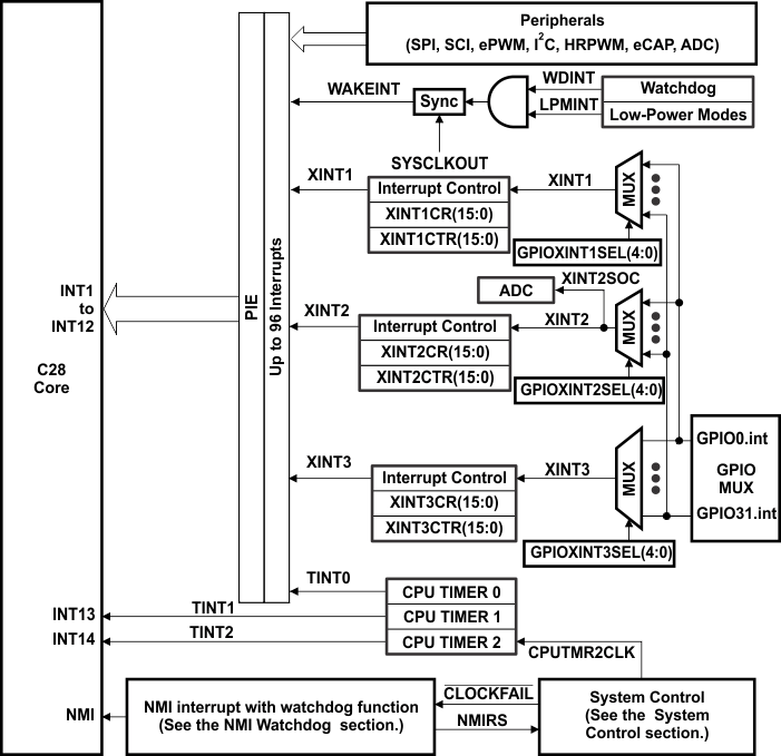
Figure 9-13 shows how the various interrupt sources are multiplexed.
 Figure 9-13 External and PIE Interrupt Sources
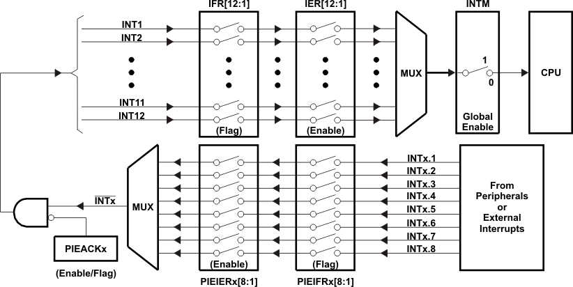
Eight PIE block interrupts are grouped into one CPU interrupt. In total, 12 CPU interrupt groups, with 8 interrupts per group equals 96 possible interrupts. Table 9-18 shows the interrupts used by 2802x devices.
The TRAP #VectorNumber instruction transfers program control to the interrupt service routine corresponding to the vector specified. The TRAP #0 instruction attempts to transfer program control to the address pointed to by the reset vector. The PIE vector table does not, however, include a reset vector. Therefore, the TRAP #0 instruction should not be used when the PIE is enabled. Doing so will result in undefined behavior.
When the PIE is enabled, the TRAP #1 to TRAP #12 instructions will transfer program control to the interrupt service routine corresponding to the first vector within the PIE group. For example: the TRAP #1 instruction fetches the vector from INT1.1, the TRAP #2 instruction fetches the vector from INT2.1, and so forth.
 Figure 9-14 Multiplexing of Interrupts Using the PIE Block
| INTx.8(1) | INTx.7 | INTx.6 | INTx.5 | INTx.4 | INTx.3 | INTx.2 | INTx.1 | |
|---|---|---|---|---|---|---|---|---|
| INT1.y | WAKEINT | TINT0 | ADCINT9 | XINT2 | XINT1 | Reserved | ADCINT2 | ADCINT1 |
| (LPM/WD) | (TIMER 0) | (ADC) | Ext. int. 2 | Ext. int. 1 | – | (ADC) | (ADC) | |
| 0xD4E | 0xD4C | 0xD4A | 0xD48 | 0xD46 | 0xD44 | 0xD42 | 0xD40 | |
| INT2.y | Reserved | Reserved | Reserved | Reserved | EPWM4_TZINT | EPWM3_TZINT | EPWM2_TZINT | EPWM1_TZINT |
| – | – | – | – | (ePWM4) | (ePWM3) | (ePWM2) | (ePWM1) | |
| 0xD5E | 0xD5C | 0xD5A | 0xD58 | 0xD56 | 0xD54 | 0xD52 | 0xD50 | |
| INT3.y | Reserved | Reserved | Reserved | Reserved | EPWM4_INT | EPWM3_INT | EPWM2_INT | EPWM1_INT |
| – | – | – | – | (ePWM4) | (ePWM3) | (ePWM2) | (ePWM1) | |
| 0xD6E | 0xD6C | 0xD6A | 0xD68 | 0xD66 | 0xD64 | 0xD62 | 0xD60 | |
| INT4.y | Reserved | Reserved | Reserved | Reserved | Reserved | Reserved | Reserved | ECAP1_INT |
| – | – | – | – | – | – | – | (eCAP1) | |
| 0xD7E | 0xD7C | 0xD7A | 0xD78 | 0xD76 | 0xD74 | 0xD72 | 0xD70 | |
| INT5.y | Reserved | Reserved | Reserved | Reserved | Reserved | Reserved | Reserved | Reserved |
| – | – | – | – | – | – | – | – | |
| 0xD8E | 0xD8C | 0xD8A | 0xD88 | 0xD86 | 0xD84 | 0xD82 | 0xD80 | |
| INT6.y | Reserved | Reserved | Reserved | Reserved | Reserved | Reserved | SPITXINTA | SPIRXINTA |
| – | – | – | – | – | – | (SPI-A) | (SPI-A) | |
| 0xD9E | 0xD9C | 0xD9A | 0xD98 | 0xD96 | 0xD94 | 0xD92 | 0xD90 | |
| INT7.y | Reserved | Reserved | Reserved | Reserved | Reserved | Reserved | Reserved | Reserved |
| – | – | – | – | – | – | – | – | |
| 0xDAE | 0xDAC | 0xDAA | 0xDA8 | 0xDA6 | 0xDA4 | 0xDA2 | 0xDA0 | |
| INT8.y | Reserved | Reserved | Reserved | Reserved | Reserved | Reserved | I2CINT2A | I2CINT1A |
| – | – | – | – | – | – | (I2C-A) | (I2C-A) | |
| 0xDBE | 0xDBC | 0xDBA | 0xDB8 | 0xDB6 | 0xDB4 | 0xDB2 | 0xDB0 | |
| INT9.y | Reserved | Reserved | Reserved | Reserved | Reserved | Reserved | SCITXINTA | SCIRXINTA |
| – | – | – | – | – | – | (SCI-A) | (SCI-A) | |
| 0xDCE | 0xDCC | 0xDCA | 0xDC8 | 0xDC6 | 0xDC4 | 0xDC2 | 0xDC0 | |
| INT10.y | ADCINT8 | ADCINT7 | ADCINT6 | ADCINT5 | ADCINT4 | ADCINT3 | ADCINT2 | ADCINT1 |
| (ADC) | (ADC) | (ADC) | (ADC) | (ADC) | (ADC) | (ADC) | (ADC) | |
| 0xDDE | 0xDDC | 0xDDA | 0xDD8 | 0xDD6 | 0xDD4 | 0xDD2 | 0xDD0 | |
| INT11.y | Reserved | Reserved | Reserved | Reserved | Reserved | Reserved | Reserved | Reserved |
| – | – | – | – | – | – | – | – | |
| 0xDEE | 0xDEC | 0xDEA | 0xDE8 | 0xDE6 | 0xDE4 | 0xDE2 | 0xDE0 | |
| INT12.y | Reserved | Reserved | Reserved | Reserved | Reserved | Reserved | Reserved | XINT3 |
| – | – | – | – | – | – | – | Ext. Int. 3 | |
| 0xDFE | 0xDFC | 0xDFA | 0xDF8 | 0xDF6 | 0xDF4 | 0xDF2 | 0xDF0 |
- No peripheral within the group is asserting interrupts.
- No peripheral interrupts are assigned to the group (for example, PIE groups 5, 7, or 11) .
| NAME | ADDRESS | SIZE (x16) | DESCRIPTION(1) |
|---|---|---|---|
| PIECTRL | 0x0CE0 | 1 | PIE, Control Register |
| PIEACK | 0x0CE1 | 1 | PIE, Acknowledge Register |
| PIEIER1 | 0x0CE2 | 1 | PIE, INT1 Group Enable Register |
| PIEIFR1 | 0x0CE3 | 1 | PIE, INT1 Group Flag Register |
| PIEIER2 | 0x0CE4 | 1 | PIE, INT2 Group Enable Register |
| PIEIFR2 | 0x0CE5 | 1 | PIE, INT2 Group Flag Register |
| PIEIER3 | 0x0CE6 | 1 | PIE, INT3 Group Enable Register |
| PIEIFR3 | 0x0CE7 | 1 | PIE, INT3 Group Flag Register |
| PIEIER4 | 0x0CE8 | 1 | PIE, INT4 Group Enable Register |
| PIEIFR4 | 0x0CE9 | 1 | PIE, INT4 Group Flag Register |
| PIEIER5 | 0x0CEA | 1 | PIE, INT5 Group Enable Register |
| PIEIFR5 | 0x0CEB | 1 | PIE, INT5 Group Flag Register |
| PIEIER6 | 0x0CEC | 1 | PIE, INT6 Group Enable Register |
| PIEIFR6 | 0x0CED | 1 | PIE, INT6 Group Flag Register |
| PIEIER7 | 0x0CEE | 1 | PIE, INT7 Group Enable Register |
| PIEIFR7 | 0x0CEF | 1 | PIE, INT7 Group Flag Register |
| PIEIER8 | 0x0CF0 | 1 | PIE, INT8 Group Enable Register |
| PIEIFR8 | 0x0CF1 | 1 | PIE, INT8 Group Flag Register |
| PIEIER9 | 0x0CF2 | 1 | PIE, INT9 Group Enable Register |
| PIEIFR9 | 0x0CF3 | 1 | PIE, INT9 Group Flag Register |
| PIEIER10 | 0x0CF4 | 1 | PIE, INT10 Group Enable Register |
| PIEIFR10 | 0x0CF5 | 1 | PIE, INT10 Group Flag Register |
| PIEIER11 | 0x0CF6 | 1 | PIE, INT11 Group Enable Register |
| PIEIFR11 | 0x0CF7 | 1 | PIE, INT11 Group Flag Register |
| PIEIER12 | 0x0CF8 | 1 | PIE, INT12 Group Enable Register |
| PIEIFR12 | 0x0CF9 | 1 | PIE, INT12 Group Flag Register |
| Reserved | 0x0CFA – 0x0CFF | 6 | Reserved |