JAJSF52 April 2018 TPA3126D2
PRODUCTION DATA.
- 1 特長
- 2 アプリケーション
- 3 概要
- 4 改訂履歴
- 5 Device Comparison Table
- 6 Pin Configuration and Functions
- 7 Specifications
-
8 Detailed Description
- 8.1 Overview
- 8.2 Functional Block Diagram
- 8.3
Feature Description
- 8.3.1 Gain Setting and Master and Slave
- 8.3.2 Input Impedance
- 8.3.3 Startup and Shutdown Operation
- 8.3.4 PLIMIT Operation
- 8.3.5 GVDD Supply
- 8.3.6 BSPx and BSNx Capacitors
- 8.3.7 Differential Inputs
- 8.3.8 Device Protection System
- 8.3.9 DC Detect Protection
- 8.3.10 Short-Circuit Protection and Automatic Recovery Feature
- 8.3.11 Thermal Protection
- 8.3.12 Device Modulation Scheme
- 8.3.13 Efficiency: LC Filter Required with the Traditional Class-D Modulation Scheme
- 8.3.14 Ferrite Bead Filter Considerations
- 8.3.15 When to Use an Output Filter for EMI Suppression
- 8.3.16 AM Avoidance EMI Reduction
- 8.4 Device Functional Modes
- 9 Application and Implementation
- 10Power Supply Recommendations
- 11Layout
- 12デバイスおよびドキュメントのサポート
- 13メカニカル、パッケージ、および注文情報
パッケージ・オプション
メカニカル・データ(パッケージ|ピン)
- DAD|32
サーマルパッド・メカニカル・データ
- DAD|32
発注情報
8.3.15 When to Use an Output Filter for EMI Suppression
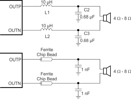
A complete LC reconstruction filter should be added in some circuit instances. These circumstances might occur if there are nearby circuits which are sensitive to noise. In these cases, a classic second order Butterworth filter similar to those shown in Figure 31 can be used.
Some systems have little power supply decoupling from the AC line but are also subject to line conducted interference (LCI) regulations. These include systems powered by "wall warts" and "power bricks." In these cases, LC reconstruction filters can be the lowest-cost methods to pass LCI tests. Common mode chokes using low frequency ferrite material can also be effective in preventing line conducted interference.
 Figure 31. Output Filters