JAJS232E November   2006  – October 2019 TPS2410 , TPS2411

PRODUCTION DATA.  

  1. 特長
  2. アプリケーション
  3. 概要
    1.     Device Images
      1.      代表的なアプリケーションの図
  4. 改訂履歴
  5. 概要(続き)
  6. Device Comparison
  7. Pin Configuration and Functions
    1.     Pin Functions, PW
    2.     Pin Functions, RMS
  8. Specifications
    1. 8.1 Absolute Maximum Ratings
    2. 8.2 ESD Ratings
    3. 8.3 Recommended Operating Conditions
    4. 8.4 Thermal Information
    5. 8.5 Electrical Characteristics: TPS2410, 11
    6. 8.6 Typical Characteristics
  9. Detailed Description
    1. 9.1 Overview
    2. 9.2 Functional Block Diagram
    3. 9.3 Feature Description
      1. 9.3.1 Device Pins
        1. 9.3.1.1  A, C:
        2. 9.3.1.2  BYP:
        3. 9.3.1.3  FLTR:
        4. 9.3.1.4  FLTB:
        5. 9.3.1.5  GATE:
        6. 9.3.1.6  GND:
        7. 9.3.1.7  RSET:
        8. 9.3.1.8  RSVD:
        9. 9.3.1.9  STAT
        10. 9.3.1.10 UV, OV, PG:
        11. 9.3.1.11 VDD:
      2. 9.3.2 Gate Drive, Charge Pump and C(BYP)
      3. 9.3.3 Fast Comparator Input Filtering – C(FLTR)
      4. 9.3.4 UV, OV, and PG
      5. 9.3.5 Input ORing and Stat
    4. 9.4 Device Functional Modes
      1. 9.4.1 TPS2410 vs TPS2411 – MOSFET Control Methods
  10. 10Application and Implementation
    1. 10.1 Typical Connections
      1. 10.1.1 N+1 Power Supply
      2. 10.1.2 Input ORing
    2. 10.2 Typical Application Examples
      1. 10.2.1 VDD, BYP, and Powering Options
      2. 10.2.2 Bidirectional Blocking and Protection of C
      3. 10.2.3 ORing Examples
      4. 10.2.4 Design Requirements
        1. 10.2.4.1 MOSFET Selection and R(RSET)
        2. 10.2.4.2 TPS2410 Regulation-loop Stability
      5. 10.2.5 Detailed Design Procedure
      6. 10.2.6 Application Curves
  11. 11Power Supply Recommendations
    1. 11.1 Recommended Operating Range
    2. 11.2 System Design and Behavior with Transients
  12. 12Layout
    1. 12.1 Layout Considerations
    2. 12.2 Layout Example
  13. 13デバイスおよびドキュメントのサポート
    1. 13.1 デバイス・サポート
    2. 13.2 関連リンク
    3. 13.3 ドキュメントの更新通知を受け取る方法
    4. 13.4 コミュニティ・リソース
    5. 13.5 商標
    6. 13.6 静電気放電に関する注意事項
    7. 13.7 Glossary
  14. 14メカニカル、パッケージ、および注文情報

パッケージ・オプション

メカニカル・データ(パッケージ|ピン)
サーマルパッド・メカニカル・データ

Typical Characteristics

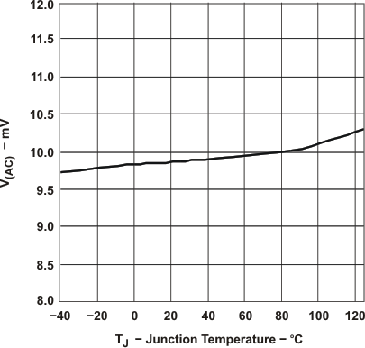
TPS2410 TPS2411 regv_v_tj_lvs727.gifFigure 1. TPS2410 V(AC) Regulation Voltage vs Temperature
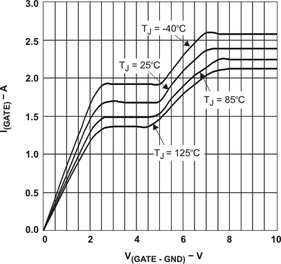
TPS2410 TPS2411 pulse_v_gatev_lvs727.gifFigure 3. Pulsed Gate Sinking Current vs Gate Voltage
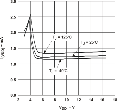
TPS2410 TPS2411 idd_v_vdd_lvs727.gifFigure 5. VDD Current vs VDD Voltage
(Gate Saturated High)
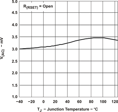
TPS2410 TPS2411 toff_v_tj_lvs727.gifFigure 2. Fast Turnoff Threshold vs Temperature
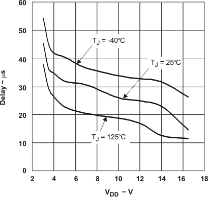
TPS2410 TPS2411 ton_v_vdd_lvs727.gifFigure 4. Turnon Delay vs VDD
(Power Applied Until Gate Is Active)