JAJS232E November   2006  – October 2019 TPS2410 , TPS2411

PRODUCTION DATA.  

  1. 特長
  2. アプリケーション
  3. 概要
    1.     Device Images
      1.      代表的なアプリケーションの図
  4. 改訂履歴
  5. 概要(続き)
  6. Device Comparison
  7. Pin Configuration and Functions
    1.     Pin Functions, PW
    2.     Pin Functions, RMS
  8. Specifications
    1. 8.1 Absolute Maximum Ratings
    2. 8.2 ESD Ratings
    3. 8.3 Recommended Operating Conditions
    4. 8.4 Thermal Information
    5. 8.5 Electrical Characteristics: TPS2410, 11
    6. 8.6 Typical Characteristics
  9. Detailed Description
    1. 9.1 Overview
    2. 9.2 Functional Block Diagram
    3. 9.3 Feature Description
      1. 9.3.1 Device Pins
        1. 9.3.1.1  A, C:
        2. 9.3.1.2  BYP:
        3. 9.3.1.3  FLTR:
        4. 9.3.1.4  FLTB:
        5. 9.3.1.5  GATE:
        6. 9.3.1.6  GND:
        7. 9.3.1.7  RSET:
        8. 9.3.1.8  RSVD:
        9. 9.3.1.9  STAT
        10. 9.3.1.10 UV, OV, PG:
        11. 9.3.1.11 VDD:
      2. 9.3.2 Gate Drive, Charge Pump and C(BYP)
      3. 9.3.3 Fast Comparator Input Filtering – C(FLTR)
      4. 9.3.4 UV, OV, and PG
      5. 9.3.5 Input ORing and Stat
    4. 9.4 Device Functional Modes
      1. 9.4.1 TPS2410 vs TPS2411 – MOSFET Control Methods
  10. 10Application and Implementation
    1. 10.1 Typical Connections
      1. 10.1.1 N+1 Power Supply
      2. 10.1.2 Input ORing
    2. 10.2 Typical Application Examples
      1. 10.2.1 VDD, BYP, and Powering Options
      2. 10.2.2 Bidirectional Blocking and Protection of C
      3. 10.2.3 ORing Examples
      4. 10.2.4 Design Requirements
        1. 10.2.4.1 MOSFET Selection and R(RSET)
        2. 10.2.4.2 TPS2410 Regulation-loop Stability
      5. 10.2.5 Detailed Design Procedure
      6. 10.2.6 Application Curves
  11. 11Power Supply Recommendations
    1. 11.1 Recommended Operating Range
    2. 11.2 System Design and Behavior with Transients
  12. 12Layout
    1. 12.1 Layout Considerations
    2. 12.2 Layout Example
  13. 13デバイスおよびドキュメントのサポート
    1. 13.1 デバイス・サポート
    2. 13.2 関連リンク
    3. 13.3 ドキュメントの更新通知を受け取る方法
    4. 13.4 コミュニティ・リソース
    5. 13.5 商標
    6. 13.6 静電気放電に関する注意事項
    7. 13.7 Glossary
  14. 14メカニカル、パッケージ、および注文情報

パッケージ・オプション

メカニカル・データ(パッケージ|ピン)
サーマルパッド・メカニカル・データ

VDD, BYP, and Powering Options

The separate VDD pin provides flexibility for operational power and controlled rail voltage. While the internal UVLO has been set to 2.5 V, the device requires at least 3 V to generate the specified GATE drive voltage. Sufficient BYP voltage to run internal circuits occurs at VDD voltages between 2.5 V and 3 V. There are three choices for power, A, C, or a separate supply, two of which are demonstrated in Figure 12. One choice for voltage rails over 3.3 V is to power from C, since it is typically the source of reliable power. Voltage rails below 3.3 V, that is, 2.5 V and below, should use a separate supply such as 5 V. A separate VDD supply can be used to control voltages above it, for example 5 V powering VDD to control a 12-V bus.

VDD is the main source of power for the internal control circuits. The charge pump that powers BYP draws most of its power from VDD. The input should be low impedance, making a bypass capacitor a preferred solution.
A 10-Ω series resistor may be used to limit inrush current into the bypass capacitor, and to provide noise filtering for the supply.

BYP is the interconnection point between a charge pump, V(AC) monitor amplifiers and comparators, and the gate driver. C(BYP) must be used to filter the charge pump. A 2200 pF is recommended, but the value is not critical.
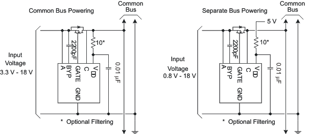
TPS2410 TPS2411 vdd_pwr_exm_lvs727.gifFigure 12. VDD Powering Examples