SLVSAL1E March 2011 – April 2016 TPS24720
PRODUCTION DATA.
- 1 Features
- 2 Applications
- 3 Description
- 4 Revision History
- 5 Pin Configuration and Functions
- 6 Specifications
-
7 Detailed Description
- 7.1 Overview
- 7.2 Functional Block Diagram
- 7.3 Feature Description
- 7.4
Device Functional Modes
- 7.4.1 Board Plug-In
- 7.4.2 Inrush Operation
- 7.4.3 Action of the Constant-Power Engine
- 7.4.4 Circuit Breaker and Fast Trip
- 7.4.5 Automatic Restart
- 7.4.6 PGb, FLTb, and Timer Operations
- 7.4.7 Overtemperature Shutdown
- 7.4.8 Start-Up of Hot-Swap Circuit by VCC or EN
- 7.4.9 Minimization of Power Dissipation at STANDY by ENSD
- 7.4.10 Fault Detection of MOSFET Short With FFLTb
-
8 Application and Implementation
- 8.1 Application Information
- 8.2
Typical Application
- 8.2.1 Design Requirements
- 8.2.2
Detailed Design Procedure
- 8.2.2.1
Power-Limited Start-Up
- 8.2.2.1.1 STEP 1. Choose RSENSE, RSET, and RIMON
- 8.2.2.1.2 STEP 2. Choose MOSFET M1
- 8.2.2.1.3 STEP 3. Choose Power-Limit Value, PLIM, and RPROG
- 8.2.2.1.4 STEP 4. Choose Output Voltage Rising Time, tON, and Timing Capacitor CT
- 8.2.2.1.5 STEP 5. Calculate the Retry-Mode Duty Ratio
- 8.2.2.1.6 STEP 6. Select R1, R2, and R3 for UV and OV
- 8.2.2.1.7 STEP 7. Choose RGATE, R4, R5, R6, and C1
- 8.2.2.2 Additional Design Considerations
- 8.2.2.1
Power-Limited Start-Up
- 8.2.3 Application Curve
- 9 Power Supply Recommendations
- 10Layout
- 11Device and Documentation Support
- 12Mechanical, Packaging, and Orderable Information
パッケージ・オプション
メカニカル・データ(パッケージ|ピン)
- RGT|16
サーマルパッド・メカニカル・データ
- RGT|16
発注情報
10 Layout
10.1 Layout Guidelines
TPS24720 applications require careful attention to layout to ensure proper performance and to minimize susceptibility to transients and noise. In general, all traces should be as short as possible, but the following list deserves first consideration:
- Decoupling capacitors on VCC pin should have minimal trace lengths to the pin and to GND.
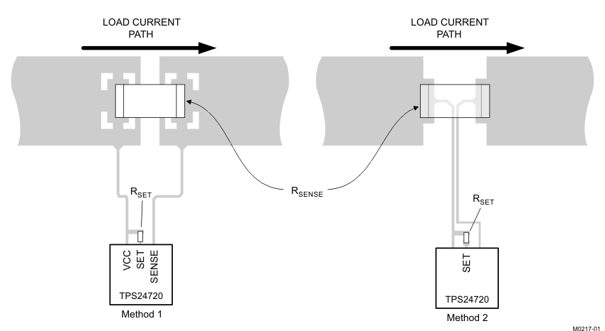
- Traces to SET and SENSE must be short and run side-by-side to maximize common-mode rejection. Kelvin connections should be used at the points of contact with RSENSE (see Figure 40).
- SET runs must be short on both sides of RSET.
- Power path connections should be as short as possible and sized to carry at least twice the full-load current, more if possible.
- Connections to GND and IMON pins should be minimized after the previously described connections have been placed.
- The device dissipates low power, so soldering the thermal pad to the board is not a requirement. However, doing so improves thermal performance and reduces susceptibility to noise.
- Protection devices such as snubbers, TVS, capacitors, or diodes should be placed physically close to the device they are intended to protect, and routed with short traces to reduce inductance. For example, the protection Schottky diode shown in the typical application diagram on the front page of the data sheet should be physically close to the OUT pin.
10.2 Layout Example
 Figure 40. Recommended RSENSE Layout