SLVSAL1E March 2011 – April 2016 TPS24720
PRODUCTION DATA.
- 1 Features
- 2 Applications
- 3 Description
- 4 Revision History
- 5 Pin Configuration and Functions
- 6 Specifications
-
7 Detailed Description
- 7.1 Overview
- 7.2 Functional Block Diagram
- 7.3 Feature Description
- 7.4
Device Functional Modes
- 7.4.1 Board Plug-In
- 7.4.2 Inrush Operation
- 7.4.3 Action of the Constant-Power Engine
- 7.4.4 Circuit Breaker and Fast Trip
- 7.4.5 Automatic Restart
- 7.4.6 PGb, FLTb, and Timer Operations
- 7.4.7 Overtemperature Shutdown
- 7.4.8 Start-Up of Hot-Swap Circuit by VCC or EN
- 7.4.9 Minimization of Power Dissipation at STANDY by ENSD
- 7.4.10 Fault Detection of MOSFET Short With FFLTb
-
8 Application and Implementation
- 8.1 Application Information
- 8.2
Typical Application
- 8.2.1 Design Requirements
- 8.2.2
Detailed Design Procedure
- 8.2.2.1
Power-Limited Start-Up
- 8.2.2.1.1 STEP 1. Choose RSENSE, RSET, and RIMON
- 8.2.2.1.2 STEP 2. Choose MOSFET M1
- 8.2.2.1.3 STEP 3. Choose Power-Limit Value, PLIM, and RPROG
- 8.2.2.1.4 STEP 4. Choose Output Voltage Rising Time, tON, and Timing Capacitor CT
- 8.2.2.1.5 STEP 5. Calculate the Retry-Mode Duty Ratio
- 8.2.2.1.6 STEP 6. Select R1, R2, and R3 for UV and OV
- 8.2.2.1.7 STEP 7. Choose RGATE, R4, R5, R6, and C1
- 8.2.2.2 Additional Design Considerations
- 8.2.2.1
Power-Limited Start-Up
- 8.2.3 Application Curve
- 9 Power Supply Recommendations
- 10Layout
- 11Device and Documentation Support
- 12Mechanical, Packaging, and Orderable Information
パッケージ・オプション
メカニカル・データ(パッケージ|ピン)
- RGT|16
サーマルパッド・メカニカル・データ
- RGT|16
発注情報
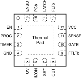
5 Pin Configuration and Functions
RGT Package
16 Pins
Top View

Pin Functions
| PIN | I/O | DESCRIPTION | |
|---|---|---|---|
| NAME | NO. | ||
| EN | 1 | I | Active-high enable input. Logic input. Connects to resistor divider. |
| ENSD | 16 | I | Pull low to put device into low-current standby mode. Logic input. |
| FFLTb | 9 | O | Active-low, open-drain FET fault indicator. Indicates shorted MOSFET when output is off. |
| FLTb | 13 | O | Active-low, open-drain output indicates overload fault timer has turned MOSFET off. |
| GATE | 10 | O | Gate driver output for external MOSFET |
| GND | 4 | – | Ground |
| IMON | 6 | O | Analog load current limit program point. Connect RIMON to ground. |
| LATCH | 14 | I | Latch or retry mode select input. Latch when floating or connected to a logic-level voltage; retry when connected to GND. |
| OUT | 8 | I | Output voltage sensor for monitoring MOSFET power. |
| OV | 5 | I | Overvoltage comparator input. Connects to resistor divider. GATE is pulled low when OV exceeds the threshold. |
| PGb | 15 | O | Active-low, open-drain power-good indicator. Status is determined by the voltage across the MOSFET. |
| PROG | 2 | I | Power-limiting programming pin. A resistor from this pin to GND sets the maximum power dissipation for the FET. |
| SENSE | 11 | I | Current-sensing input for resistor shunt from VCC to SENSE. |
| SET | 7 | I | Current-limit programming set pin. A resistor is connected from this pin to VCC. |
| TIMER | 3 | I/O | A capacitor connected from this pin to GND provides a fault timing function. |
| VCC | 12 | I | Input-voltage sense and power supply |
| Thermal pad | — | — | Tied to GND |