SLVSAL1E March 2011 – April 2016 TPS24720
PRODUCTION DATA.
- 1 Features
- 2 Applications
- 3 Description
- 4 Revision History
- 5 Pin Configuration and Functions
- 6 Specifications
-
7 Detailed Description
- 7.1 Overview
- 7.2 Functional Block Diagram
- 7.3 Feature Description
- 7.4
Device Functional Modes
- 7.4.1 Board Plug-In
- 7.4.2 Inrush Operation
- 7.4.3 Action of the Constant-Power Engine
- 7.4.4 Circuit Breaker and Fast Trip
- 7.4.5 Automatic Restart
- 7.4.6 PGb, FLTb, and Timer Operations
- 7.4.7 Overtemperature Shutdown
- 7.4.8 Start-Up of Hot-Swap Circuit by VCC or EN
- 7.4.9 Minimization of Power Dissipation at STANDY by ENSD
- 7.4.10 Fault Detection of MOSFET Short With FFLTb
-
8 Application and Implementation
- 8.1 Application Information
- 8.2
Typical Application
- 8.2.1 Design Requirements
- 8.2.2
Detailed Design Procedure
- 8.2.2.1
Power-Limited Start-Up
- 8.2.2.1.1 STEP 1. Choose RSENSE, RSET, and RIMON
- 8.2.2.1.2 STEP 2. Choose MOSFET M1
- 8.2.2.1.3 STEP 3. Choose Power-Limit Value, PLIM, and RPROG
- 8.2.2.1.4 STEP 4. Choose Output Voltage Rising Time, tON, and Timing Capacitor CT
- 8.2.2.1.5 STEP 5. Calculate the Retry-Mode Duty Ratio
- 8.2.2.1.6 STEP 6. Select R1, R2, and R3 for UV and OV
- 8.2.2.1.7 STEP 7. Choose RGATE, R4, R5, R6, and C1
- 8.2.2.2 Additional Design Considerations
- 8.2.2.1
Power-Limited Start-Up
- 8.2.3 Application Curve
- 9 Power Supply Recommendations
- 10Layout
- 11Device and Documentation Support
- 12Mechanical, Packaging, and Orderable Information
パッケージ・オプション
メカニカル・データ(パッケージ|ピン)
- RGT|16
サーマルパッド・メカニカル・データ
- RGT|16
発注情報
6 Specifications
6.1 Absolute Maximum Ratings
over operating free-air temperature range, all voltages referred to GND (unless otherwise noted)| MIN | MAX | UNIT | |||
|---|---|---|---|---|---|
| Input voltage range | EN, FFLTb(1), FLTb(1), GATE, OUT, PGb(1), SENSE, SET(1), VCC | –0.3 | 30 | V | |
| ENSD, OV | –0.3 | 20 | |||
| PROG(1) | –0.3 | 3.6 | |||
| [SET, SENSE] to VCC | –0.3 | 0.3 | |||
| IMON, LATCH, TIMER | –0.3 | 5 | |||
| Sink current | FFLTb, FLTb, PGb | 5 | mA | ||
| Source current | PROG | Internally limited | |||
| IMON | 5 | mA | |||
| Temperature | Maximum junction, TJ | Internally limited | °C | ||
(1) Do not apply voltage directly to these pins.
6.2 ESD Ratings
| VALUE | UNIT | ||||
|---|---|---|---|---|---|
| V(ESD) | Electrostatic discharge | Human-body model (HBM), per ANSI/ESDA/JEDEC JS-001(1) | All pins except PGb | ±2000 | V |
| PIN PGb | ±500 | V | |||
| Charged-device model (CDM), per JEDEC specification JESD22-C101(2) | ±500 | V | |||
(1) JEDEC document JEP155 states that 500-V HBM allows safe manufacturing with a standard ESD control process.
(2) JEDEC document JEP157 states that 250-V CDM allows safe manufacturing with a standard ESD control process.
6.3 THERMAL INFORMATION
| THERMAL METRIC(1) | TPS24720 | UNIT | |
|---|---|---|---|
| QFN (16) PINS | |||
| RθJA | Junction-to-ambient thermal resistance | 47.3 | °C/W |
| RθJCtop | Junction-to-case (top) thermal resistance | 63.8 | °C/W |
| RθJB | Junction-to-board thermal resistance | 20.9 | °C/W |
| ψJT | Junction-to-top characterization parameter | 1.6 | °C/W |
| ψJB | Junction-to-board characterization parameter | 21 | °C/W |
| RθJCbot | Junction-to-case (bottom) thermal resistance | 5.1 | °C/W |
(1) For more information about traditional and new thermal metrics, see the Semiconductor and IC Package Thermal Metrics application report (SPRA953).
6.4 Recommended Operating Conditions
over operating free-air temperature range (unless otherwise noted)| MIN | NOM | MAX | UNIT | ||
|---|---|---|---|---|---|
| Input voltage range | ENSD, OV | 0 | 16 | V | |
| SENSE, SET(1), VCC | 2.5 | 18 | |||
| EN, FFLTb, FLTb, PGb, OUT | 0 | 18 | |||
| Sink current | FFLTb, FLTb, PGb | 0 | 2 | mA | |
| Source current | IMON | 0 | 1 | mA | |
| Resistance | PROG | 4.99 | 500 | kΩ | |
| External capacitance | TIMER | 1 | nF | ||
| Operating junction temperature range, TJ | –40 | 125 | °C | ||
(1) Do not apply voltage directly to these pins.
6.5 Electrical Characteristics
–40°C ≤ TJ ≤ 125°C, VCC = 12 V, VEN = 3 V, VENSD = 3 V, RSET = 190 Ω, RIMON = 5 kΩ, and RPROG = 50 kΩ to GND.All voltages referenced to GND, unless otherwise noted.
| PARAMETER | CONDITIONS | MIN | NOM | MAX | UNIT |
|---|---|---|---|---|---|
| VCC | |||||
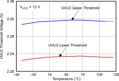
| UVLO threshold, rising | 2.2 | 2.32 | 2.45 | V | |
| UVLO threshold, falling | 2.1 | 2.22 | 2.35 | V | |
| UVLO hysteresis(1) | 0.1 | V | |||
| Supply current | Enabled ― IOUT + IVCC + ISENSE | 1 | 1.4 | mA | |
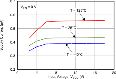
| Disabled (1) ― EN = 0 V, IOUT + IVCC + ISENSE | 0.45 | mA | |||
| Shutdown ― ENSD = 0 V, IOUT + IVCC + ISENSE | 1.7 | 10 | µA | ||
| EN | |||||
| Threshold voltage, falling | 1.2 | 1.3 | 1.4 | V | |
| Hysteresis(1) | 50 | mV | |||
| Input leakage current | 0 V ≤ VEN ≤ 30 V | –1 | 0 | 1 | µA |
| ENSD | |||||
| Threshold voltage | Rising or falling edge | 0.3 | 0.7 | 1.4 | V |
| Pullup current | VENSD = 5 V | 0.5 | 1.2 | 2 | µA |
| OV | |||||
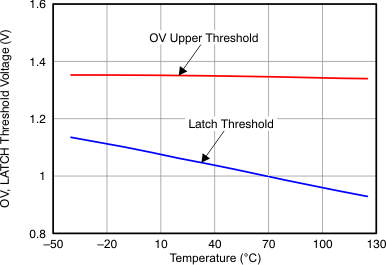
| Threshold voltage, rising | 1.25 | 1.35 | 1.45 | V | |
| Hysteresis(1) | 60 | mV | |||
| Input leakage current | 0 V ≤ VOV ≤ 30 V | –1 | 0 | 1 | µA |
| Deglitch time | OV rising | 0.5 | 1.2 | 1.5 | µs |
| FLTb | |||||
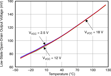
| Output low voltage | Sinking 2 mA | 0.11 | 0.25 | V | |
| Input leakage current | VFLTb = 0 V, 30 V | –1 | 0 | 1 | µA |
| PGb | |||||
| Threshold | V(SENSE – OUT) rising, PGb going high | 140 | 240 | 340 | mV |
| Hysteresis(1) | Measured V(SENSE – OUT) falling, PGb going low | 70 | mV | ||
| Output low voltage | Sinking 2 mA | 0.11 | 0.25 | V | |
| Input leakage current | VPGb = 0 V, 30 V | –1 | 0 | 1 | µA |
| FFLTb | |||||
| VIMON threshold | Measured VIMON to GND | 90 | 103 | 115 | mV |
| Output low voltage | Sinking 2 mA | 0.11 | 0.25 | V | |
| Input leakage current | FFLTb = 0 V, 30 V | –1 | 0 | 1 | µA |
| PROG | |||||
| Bias voltage | Sourcing 10 µA | 0.65 | 0.678 | 0.7 | V |
| Input leakage current | VPROG = 1.5 V | –0.2 | 0 | 0.2 | µA |
| TIMER | |||||
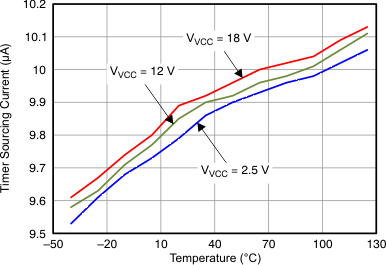
| Sourcing current | VTIMER = 0 V | 8 | 10 | 12 | µA |
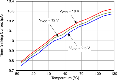
| Sinking current | VTIMER = 2 V | 8 | 10 | 12 | µA |
| VEN = 0 V, VTIMER = 2 V | 2 | 4.5 | 7 | mA | |
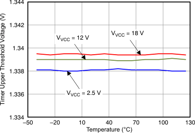
| Upper threshold voltage | 1.3 | 1.35 | 1.4 | V | |
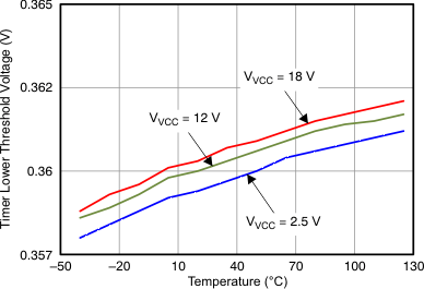
| Lower threshold voltage | 0.33 | 0.35 | 0.37 | V | |
| Timer activation voltage | Raise GATE until ITIMER sinking, measure V(GATE – VCC), VVCC = 12 V | 5 | 5.9 | 7 | V |
| Bleed-down resistance | VENSD = 0 V, VTIMER = 2 V | 70 | 104 | 130 | kΩ |
| IMON | |||||
| Summing threshold | Current limit in regulation | 660 | 675 | 690 | mV |
| OUT | |||||
| Input bias current | VOUT = 12 V | 16 | 30 | µA | |
| SET | |||||
| Input referred offset | Measure SET to SENSE | –1.5 | 0 | 1.5 | mV |
| GATE | |||||
| Output voltage | VOUT = 12 V | 23.5 | 25.8 | 28 | V |
| Clamp voltage | Inject 10 µA into GATE, measure V(GATE – VCC) | 12 | 13.9 | 15.5 | V |
| Sourcing current | VGATE = 12 V | 20 | 30 | 40 | µA |
| Sinking current | Fast turnoff, VGATE = 14 V | 0.5 | 1 | 1.4 | A |
| Sustained, VGATE = 4 V to 23 V | 6 | 11 | 20 | mA | |
| In inrush current limit, VGATE = 4 V to 23 V | 20 | 30 | 40 | µA | |
| Pulldown resistance | Thermal shutdown or VENSD = 0 V | 14 | 20 | 26 | kΩ |
| SENSE | |||||
| Input bias current | VSENSE = 12 V, sinking current | 30 | 40 | µA | |
| Current limit threshold | VOUT = 12 V | 22.5 | 25 | 27.5 | mV |
| Power limit threshold | VOUT = 7 V, RPROG = 50 kΩ | 10 | 12.5 | 15 | mV |
| VOUT = 2 V, RPROG = 25 kΩ | 10 | 12.5 | 15 | ||
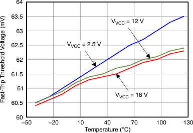
| Fast-trip threshold | 52 | 60 | 68 | mV | |
| LATCH | |||||
| Threshold, rising | 0.3 | 0.9 | 1.4 | V | |
| Pullup current | VLATCH = 0 V | 7 | 10 | 13 | µA |
| OTSD | |||||
| Threshold, rising | 130 | 140 | °C | ||
| Hysteresis(1) | 10 | °C | |||
(1) Parameters are provided for reference only, and do not constitute part of TI’s published specifications for purposes of TI product warranty.
6.6 Timing Requirements
| MIN | NOM | MAX | UNIT | ||
|---|---|---|---|---|---|
| EN | |||||
| Turnoff time | EN ↓ to VGATE < 1 V, CGATE = 33 nF | 20 | 60 | 150 | µs |
| Deglitch time | EN ↑ | 8 | 14 | 18 | µs |
| Disable delay | EN ↓ to GATE ↓, CGATE = 0, tpff50–90, See Figure 1 | 0.1 | 0.4 | 1 | µs |
| ENSD | |||||
| Disable delay | ENSD to GATE, tpff50–90, See Figure 1 | 0.75 | 1 | µs | |
| FFLTb | |||||
| Delay | FFLTb falling | 60 | 115 | 140 | ms |
| PG, PGb | |||||
| Delay (deglitch) time | Rising or falling edge | 2 | 3.4 | 6 | ms |
| GATE | |||||
| Turn on delay | VVCC rising to GATE sourcing, tprr50-50, See Figure 3 | 100 | 250 | µs | |
| SENSE | |||||
| Fast-turnoff duration | 8 | 13.5 | 18 | µs | |
| Fast-turnoff delay (1) | V(VCC – SENSE) = 80 mV, CGATE = 0 pF, tprf50–50, See Figure 4 | 200 | ns | ||
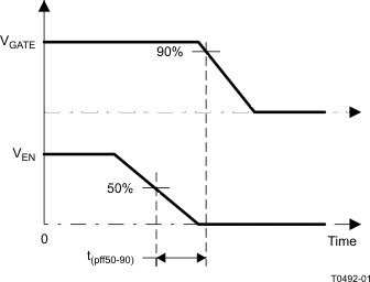 Figure 1. tpff50–90 Timing Definition
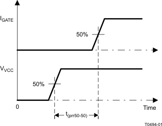 Figure 3. tprr50–50 Timing Definition
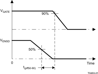 Figure 2. tpff50–90 Timing Definition
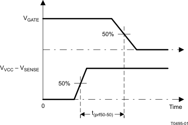 Figure 4. tprf50–50 Timing Definition
6.7 Typical Characteristics
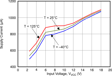
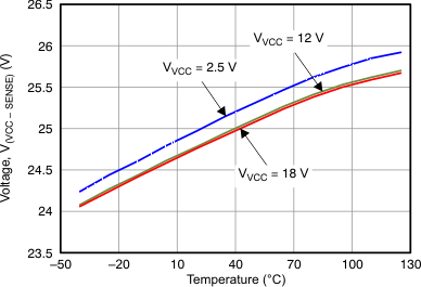
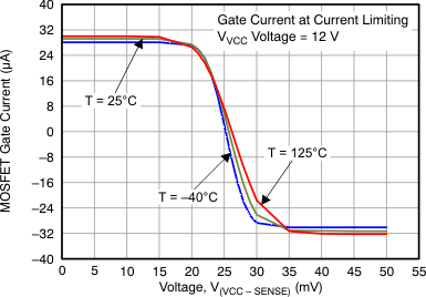
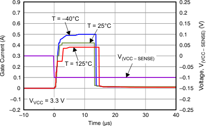
VVCC = VGATE = 3.3 V
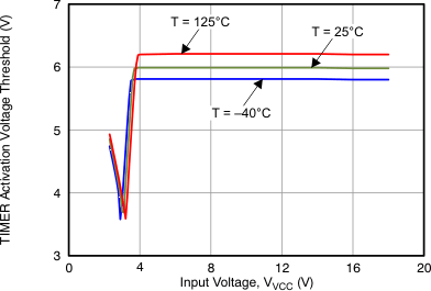
vs Input Voltage at Various Temperatures
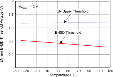
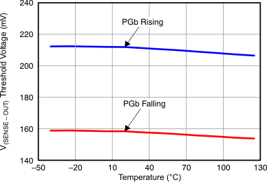
PGb Rising and Falling

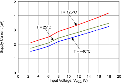
(EN = 0 V)
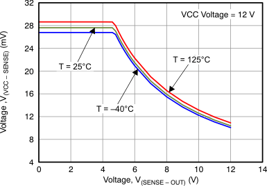
vs VDS of Pass MOSFET
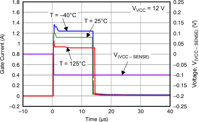
VVCC = VGATE = 12 V
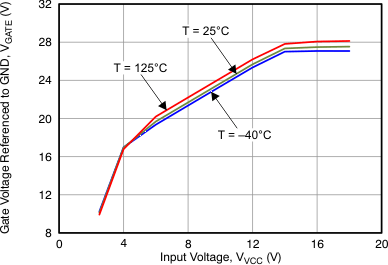
vs Input Voltage
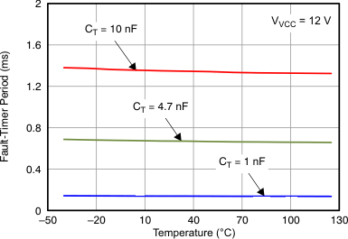
TIMER Capacitors
