JAJSGC8B October 2018 – January 2020 TPS25982
PRODUCTION DATA.
- 1 特長
- 2 アプリケーション
- 3 概要
- 4 改訂履歴
- 5 デバイス比較表
- 6 概要 (続き)
- 7 Pin Configuration and Functions
- 8 Specifications
-
9 Detailed Description
- 9.1 Overview
- 9.2 Functional Block Diagram
- 9.3 Feature Description
- 9.4 Fault Response
- 9.5 Device Functional Modes
-
10Application and Implementation
- 10.1 Application Information
- 10.2
Typical Application: Standby Power Rail Protection in Datacenter Servers
- 10.2.1 Design Requirements
- 10.2.2
Detailed Design Procedure
- 10.2.2.1 Device Selection
- 10.2.2.2 Setting the Current Limit Threshold: RILIM Selection
- 10.2.2.3 Setting the Undervoltage Lockout Set Point
- 10.2.2.4 Choosing the Current Monitoring Resistor: RIMON
- 10.2.2.5 Setting the Output Voltage Ramp Time (TdVdt)
- 10.2.2.6 Setting the Load Handshake (LDSTRT) Delay
- 10.2.2.7 Setting the Transient Overcurrent Blanking Interval (tITIMER)
- 10.2.2.8 Setting the Auto-Retry Delay and Number of Retries
- 10.2.3 Application Curves
- 10.3 System Examples
- 11Power Supply Recommendations
- 12Layout
- 13デバイスおよびドキュメントのサポート
- 14メカニカル、パッケージ、および注文情報
パッケージ・オプション
メカニカル・データ(パッケージ|ピン)
- RGE|24
サーマルパッド・メカニカル・データ
- RGE|24
発注情報
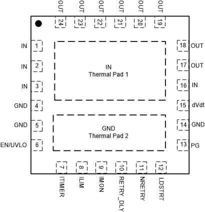
7 Pin Configuration and Functions
RGE
24-Pin QFN
Top View

Pin Functions
| PIN | TYPE | DESCRIPTION | |
|---|---|---|---|
| NAME | NO. | ||
| OUT | 17, 18, 19, 20, 21, 22, 23, 24 | Power | Power Output |
| IN | 1, 2, 3, 16, Pad 1 | Thermal / Power | Power Input. The exposed pad must be soldered to input power plane uniformly to ensure proper heat dissipation and to maintain optimal current distribution through the device. |
| GND | 4, 5, 14,
Pad 2 |
Ground | Connect to System Ground |
| EN/UVLO | 6 | Analog Input | Active High Enable for the device. A resistor divider on this pin from input supply to GND can be used to adjust the Undervoltage Lockout threshold. Do not leave floating. |
| ITIMER | 7 | Analog Output | A capacitor from this pin to GND sets the overcurrent blanking interval during which the output current can temporarily exceed set current limit (but lower than fast-trip threshold) before the device overcurrent response takes action. Leave this pin open for fastest response to overcurrent events. Refer to ITIMER Functional Mode Summary for more details. |
| ILIM | 8 | Analog Output | An external resistor from this pin to GND sets the output current limit threshold and fast trip threshold. Do not leave floating. |
| IMON | 9 | Analog Output | Analog output load current monitor. This pin sources a current proportional to the load current. This can be converted to a voltage signal by connecting an appropriate resistor from this pin to GND. |
| RETRY_DLY | 10 | Analog Output | A capacitor from this pin to GND sets the time period that has to elapse after a fault shutdown before the device attempts to restart automatically. Connect this pin to GND for latch-off operation (no auto-retries) after a fault. Refer to Fault Response section for more details. |
| NRETRY | 11 | Analog Output | A capacitor from this pin to GND sets the number of times the part attempts to restart automatically after shutdown due to fault. Connect this pin to GND if the part should retry indefinitely. Refer to Fault Response section for more details. |
| LDSTRT | 12 | Analog Input | Load Detect/Handshake Signal. A capacitor from this pin to GND sets the time period after PG assertion within which the pin has to be pulled low for the device to remain ON. Connect to GND if the load detect/handshake feature is not used. Refer to Load Detect/Handshake (LDSTRT) section for more details. Do not leave floating. |
| PG | 13 | Digital Output | Active High Power Good Indication. This pin is asserted when the FET is fully enhanced and output has reached maximum voltage. It is an open drain output that requires an external pull-up resistor to an external supply. This pin remains logic low when VIN < VUVP. |
| dVdt | 15 | Analog Output | A capacitor from this pin to GND sets the output turn on slew rate. Leave this pin floating for the fastest slew rate during start up. |