SLUSBW8 September 2014 TPS53632
PRODUCTION DATA.
- 1 Features
- 2 Applications
- 3 Description
- 4 Revision History
- 5 Pin Configuration and Functions
- 6 Specifications
-
7 Detailed Description
- 7.1 Overview
- 7.2 Functional Block Diagram
- 7.3
Feature Description
- 7.3.1 Current Sensing
- 7.3.2 Load Transients
- 7.3.3 AutoBalance Current Sharing
- 7.3.4 PWM and SKIP Signals
- 7.3.5 5-V, 3.3-V and 1.8-V Undervoltage Lockout (UVLO)
- 7.3.6 Output Undervoltage Protection (UVP)
- 7.3.7 Overcurrent Protection (OCP)
- 7.3.8 Overvoltage Protection
- 7.3.9 Analog Current Monitor, IMON and Corresponding Digital Output Current
- 7.3.10 Addressing
- 7.3.11 I2C Interface Operation
- 7.3.12 Start-Up Sequence
- 7.3.13 Phase Add and Drop Operation
- 7.3.14 Power Good Operation
- 7.3.15 Input Voltage Limits
- 7.3.16 Fault Behavior
- 7.4 Device Functional Modes
- 7.5 Configuration and Programming
- 7.6 Register Maps
-
8 Applications and Implementation
- 8.1
Application Information
- 8.1.1
3-Phase D-CAP+™, Step-Down Application
- 8.1.1.1 Design Requirements
- 8.1.1.2
Detailed Design Procedure
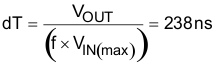
- 8.1.1.2.1 Step 1: Select Switching Frequency
- 8.1.1.2.2 Step 2: Set The Slew Rate
- 8.1.1.2.3 Step 3: Determine Inductor Value And Choose Inductor
- 8.1.1.2.4 Step 4: Determine Current Sensing Method
- 8.1.1.2.5 Step 5: DCR Current Sensing
- 8.1.1.2.6 Step 6: Select OCP Level
- 8.1.1.2.7 Step 7: Set the Load-Line Slope
- 8.1.1.2.8 Step 8: Current Monitor (IMON) Setting
- 8.1.1.3 Application Performance Plots
- 8.1.1.4 Loop Compensation for Zero Load-Line
- 8.1.1
3-Phase D-CAP+™, Step-Down Application
- 8.1
Application Information
- 9 Power Supply Recommendations
- 10 Layout
- 11Device and Documentation Support
- 12Mechanical, Packaging, and Orderable Information
8 Applications and Implementation
8.1 Application Information
The TPS53632 device has a very simple design procedure. A Microsoft Excel®-based component value calculation tool is available. Please contact your local TI representative to get a copy of the spreadsheet.
Typical Application
8.1.1 3-Phase D-CAP+™, Step-Down Application
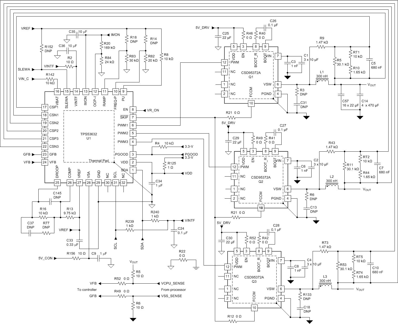 Figure 22. 3-Phase D-CAP+™, Step-Down Application with Power Stages
8.1.1.1 Design Requirements
Design example specifications:
- Number of phases: 3
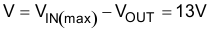
- Input voltage range: 10 V to 14 V
- VOUT = 1.0 V
- ICC(max) = 80 A
- Slew rate (minimum): 12 mV/µs
- Load-line = 1 mΩ
8.1.1.2 Detailed Design Procedure
8.1.1.2.1 Step 1: Select Switching Frequency
The switching frequency is selected by a resistor (RF) between the FREQ_P pin and GND. The frequency is approximate and expected to vary based on load and input voltage.
Table 3. TPS53632 Device Frequency Selection Table
| SELECTION RESISTOR (RF) VALUE (kΩ) |
OPERATING FREQUENCY (fSW) (kHz) |
|---|---|
| 20 | 300 |
| 24 | 400 |
| 30 | 500 |
| 39 | 600 |
| 56 | 700 |
| 75 | 800 |
| 100 | 900 |
| 150 | 1000 |
For this design, choose a switching frequency of 300 kHz. So, RF = 20 kΩ.
8.1.1.2.2 Step 2: Set The Slew Rate
A resistor to GND (RSLEWA) on SLEWA pin sets the slew rate. For a minimum 12 mV/µs slew rate, the resistor RSLEWA = 24 kΩ.
Table 4. Slew Rate Versus Selection Resistor
| SELECTION RESISTOR RSLEWA (kΩ) |
MINIMUM SLEW RATE (mV/µs) |
|---|---|
| 20 | 6 |
| 24 | 12 |
| 30 | 18 |
| 39 | 24 |
| 56 | 30 |
| 75 | 36 |
| 100 | 42 |
| 150 | 48 |
NOTE
The voltage on the SLEWA pin also sets the base address. For a base address of 00, the SLEWA pin should have only one resistor, RSLEW to GND. For other base addresses, a resistor can be connected between the SLEWA pin and the VREF pin (1.7 V). This resistor can be calculated to set the corresponding voltage for the required address listed in Table 5.
Table 5. Address Selection
| SLEWA VOLTAGE |
BASE ADDRESS |
|---|---|
| VSLEWA ≤ 0.30 V | 0 |
| 0.35 V ≤ VSLEWA ≤ 0.45 V | 1 |
| 0.55 V ≤ VSLEWA ≤ 0.65 V | 2 |
| 0.75 V ≤ VSLEWA ≤ 0.85 V | 3 |
| 0.95 V ≤ VSLEWA ≤ 1.05 V | 4 |
| 1.15 V ≤ VSLEWA ≤ 1.25 V | 5 |
| 1.35 V ≤ VSLEWA ≤ 1.45 V | 6 |
| 1.55 V ≤ VSLEWA ≤ 1.65 V | 7 |
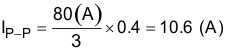
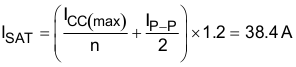
8.1.1.2.3 Step 3: Determine Inductor Value And Choose Inductor
Applications with smaller inductor values have better transient performance but also have higher voltage ripple and lower efficiency. Applications with higher inductor values have the opposite characteristics. It is common practice to limit the ripple current between 20% and 40% of the maximum current per phase. In this case, use 30%.

In this equation,
So, calculating, L = 0.29 µH.
Choose an inductance value of 0.3 µH. The inductor must not saturate during peak loading conditions.
where
- n is the number of phases
The factor of 1.2 allows for current sensing and current limiting tolerances.
The chosen inductor should have the following characteristics:
- As flat as an inductance versus current curve as possible. Inductor DCR sensing is based on the idea L / DCR is approximately a constant through the current range of interest
- Either high saturation or soft saturation
- Low DCR for improved efficiency, but at least 0.6 mΩ for proper signal levels
- DCR tolerance as low as possible for load-line accuracy
For this application, choose a 0.3-µH, 0.29-mΩ inductor.
8.1.1.2.4 Step 4: Determine Current Sensing Method
The TPS53632 device supports both resistor sensing and inductor DCR sensing. Inductor DCR sensing is chosen. For resistor sensing, substitute the resistor value for RCS(eff) in the subsequent equations.
8.1.1.2.5 Step 5: DCR Current Sensing
Design the thermal compensation network and selection of OCP. In most designs, NTC thermistors are used to compensate thermal variations in the resistance of the inductor winding. This winding is generally copper, and so has a resistance coefficient of 3900 PPM/°C. NTC thermistors, as an alternative, have very non-linear characteristics and need two or three resistors to linearize them over the range of interest. A typical DCR circuit is shown in Figure 23.
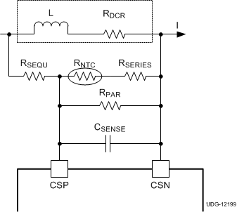 Figure 23. Typical DCR Sensing Circuit
In this design example, the voltage across the CSENSE capacitor exactly equals the voltage across RDCR when:


where
- REQ is the series (or parallel) combination of RSEQU, RNTC, RSERIES and RPAR

Ensure that CSENSE is a capacitor type which is stable over temperature. Use X7R or better dielectric (C0G preferred).
Because calculating these values by hand is difficult, TI offers a spreadsheet using the Excel solver function available to calculate them for you. Contact a TI representative to get a copy of the spreadsheet.
In this design, the following values are input to the spreadsheet.
- L = 0.3 µH
- RDCR = 0.29 mΩ
- Minimum Overcurrent Limit = 110 A
- Thermistor R25 = 10 kΩ and “B” value = 3380 kΩ
The spreadsheet then calculates the OCP setting and the values of RSEQU, RSERIES, RPAR, and CSENSE. In this case, the OCP setting is the value of the resistor that is conencted between the OCP-I pin and GND. (100 kΩ ) The nearest standard component values are:
- RSEQU = 1.47 kΩ
- RSERIES = 1.65 kΩ
- RPAR = 30.1 kΩ
- CSENSE = 680 nF
Consider the effective divider ratio for the inductor DCR. Equation 10 shows the effective current sense resistance (RCS(eff) calculation.

RP_N is the series and parallel combination of RNTC, RSERIES, and RPAR.
RCS(eff) is 0.244 mΩ.
8.1.1.2.6 Step 6: Select OCP Level
Set the OCP threshold level that corresponds to Equation 12.


Table 6. OCP Selection(1)
| SELECTION RESISTOR ROCP (kΩ) |
TYPICAL VCS(OCP)
(mV) |
|---|---|
| 20 | 4 |
| 24 | 8 |
| 30 | 13 |
| 39 | 19 |
| 56 | 25 |
| 75 | 32 |
| 100 | 40 |
| 150 | 49 |
8.1.1.2.7 Step 7: Set the Load-Line Slope
The load-line slope is set by resistor, RDROOP (between the DROOP pin and the COMP pin) and resistor RCOMP (between the COMP pin and the VREF pin). The gain of the DROOP amplifier (ADROOP) is calculated in Equation 14.
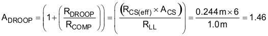
Set the value of RDROOP to 10 kΩ, RCOMP as shown in Equation 15.
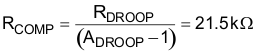
Based on measurement, this value is adjusted to 9.75 kΩ.
NOTE
See Loop Compensation for Zero Load-Line for zero-load line.
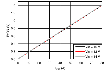
8.1.1.2.8 Step 8: Current Monitor (IMON) Setting
Set the analog current monitor so that at ICC(max) the IMON pin voltage is 1.7 V. This corresponds to a digital IOUT value of ‘FF’ in I2C register 03H. The voltage on the IMON pin is shown in Equation 16.
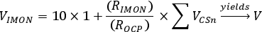
So,

where
- ICC(max)is 80 A
- RCS(eff) is 0.244 mΩ
- ROCP is 24 kΩ
Solving, RIMON = 169 kΩ. RIMON is connected from IMON pin to OCP-I pin.
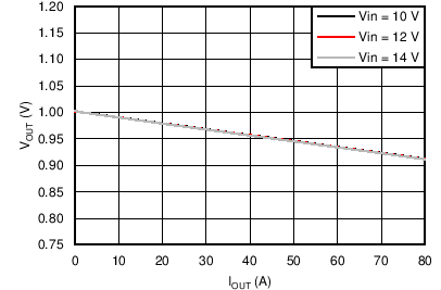
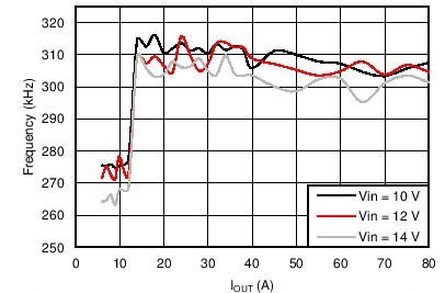
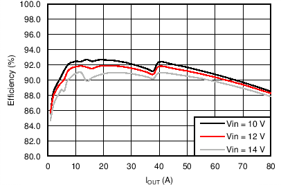
8.1.1.3 Application Performance Plots
8.1.1.4 Loop Compensation for Zero Load-Line
The TPS53632 device control architecture (current mode, constant on-time) has been analyzed by the Center for Power Electronics Systems (CPES) at Virginia Polytechnic and State University. The following equations are from the presentation: Equivalent Circuit Representation of Current-Mode Control from November 21, 2008.
A simplified control loop diagram is shown in Figure 28. One of the benefits of this technology is the lack of the sample and hold effect that limits the bandwidth of fixed frequency current mode controllers and causes sub-harmonic oscillations.
The open loop gain, GOL, is the gain of the error amplifier, multiplied by the control-to-output gain and is calculated in Equation 18.

The control-to-output gain circuitry is shown in Figure 28.
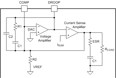 Figure 28. Control To Output Gain Circuitry
The control-to-output gain is calculated in Equation 19.

where


For this converter, Ri = RCS(eff) × ACS
The theoretical control-to-output transfer function shows 0-dB bandwidth is approximately 20 kHz and the phase margin is greater than 90°. As a result, creating the desired loop response is a matter of adding an appropriate pole-zero or pole-zero-pole compensation for the high-gain system.
The loop compensation is designed to meet the following criteria:
- Phase margin ≥ 60°
- More stable and settles more quickly for repetitive transients
- Bandwidth:

- High-enough BW for good transient response.
- If too high, the response for the voltage changes gets very “bumpy”, as each voltage step causes several pulses very quickly.
- The phase angle of the compensation at the switching frequency needs to be very near to 0 degrees (resistive)
- Otherwise, there is a phase shift between DROOP and ISUM
- Practically, this means the zero frequency should be < fSW / 2, and any high-frequency pole (for noise rejection) needs to be > 2 × fSW.
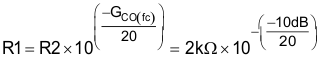
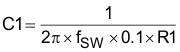
The voltage error amplifier is used in the design. The compensation technique used here is a type II compensator. Equation 20 describes the transfer function, which has a pole that occurs at the origin. The type II amplifier also has a 0 (fZ) that can be programmed by selecting R1 and C1 values. In addition, the type II compensation network has a pole (fP) that can be programmed by selecting R1 and C2.


R1 sets the loop crossover to correct for the gain at control to output function. In this design, select R2 = 2 kΩ.
Capacitor C1 adds phase margin at crossover frequency and can be set between 10% and 20% of the switching frequency.
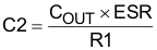
The last consideration for the voltage loop compensation design is C2. The purpose of C2 is to cancel the phase gain caused by the ESR of the output capacitor in the control-to-output function after the loop crossover. To ensure the gain continues to roll off after the voltage loop crossover, the C2 is selected to meet Equation 25.