SLUSBW8 September 2014 TPS53632
PRODUCTION DATA.
- 1 Features
- 2 Applications
- 3 Description
- 4 Revision History
- 5 Pin Configuration and Functions
- 6 Specifications
-
7 Detailed Description
- 7.1 Overview
- 7.2 Functional Block Diagram
- 7.3
Feature Description
- 7.3.1 Current Sensing
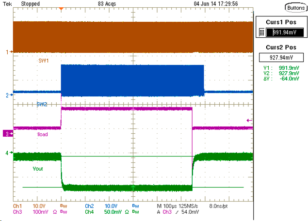
- 7.3.2 Load Transients
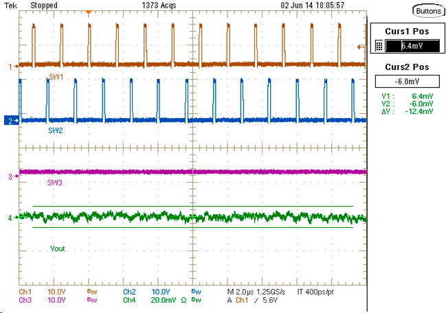
- 7.3.3 AutoBalance Current Sharing
- 7.3.4 PWM and SKIP Signals
- 7.3.5 5-V, 3.3-V and 1.8-V Undervoltage Lockout (UVLO)
- 7.3.6 Output Undervoltage Protection (UVP)
- 7.3.7 Overcurrent Protection (OCP)
- 7.3.8 Overvoltage Protection
- 7.3.9 Analog Current Monitor, IMON and Corresponding Digital Output Current
- 7.3.10 Addressing
- 7.3.11 I2C Interface Operation
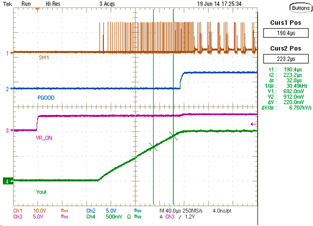
- 7.3.12 Start-Up Sequence
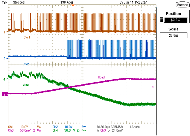
- 7.3.13 Phase Add and Drop Operation
- 7.3.14 Power Good Operation
- 7.3.15 Input Voltage Limits
- 7.3.16 Fault Behavior
- 7.4 Device Functional Modes
- 7.5 Configuration and Programming
- 7.6 Register Maps
-
8 Applications and Implementation
- 8.1
Application Information
- 8.1.1
3-Phase D-CAP+™, Step-Down Application
- 8.1.1.1 Design Requirements
- 8.1.1.2
Detailed Design Procedure
- 8.1.1.2.1 Step 1: Select Switching Frequency
- 8.1.1.2.2 Step 2: Set The Slew Rate
- 8.1.1.2.3 Step 3: Determine Inductor Value And Choose Inductor
- 8.1.1.2.4 Step 4: Determine Current Sensing Method
- 8.1.1.2.5 Step 5: DCR Current Sensing
- 8.1.1.2.6 Step 6: Select OCP Level
- 8.1.1.2.7 Step 7: Set the Load-Line Slope
- 8.1.1.2.8 Step 8: Current Monitor (IMON) Setting
- 8.1.1.3 Application Performance Plots
- 8.1.1.4 Loop Compensation for Zero Load-Line
- 8.1.1
3-Phase D-CAP+™, Step-Down Application
- 8.1
Application Information
- 9 Power Supply Recommendations
- 10 Layout
- 11Device and Documentation Support
- 12Mechanical, Packaging, and Orderable Information
6 Specifications
6.1 Absolute Maximum Ratings
over operating free-air temperature range (unless otherwise noted) (1)| MIN | MAX | UNIT | ||
|---|---|---|---|---|
| Input voltage | PWM3, PWM2, PWM1, SKIP, V5A | –0.3 | 6.0 | V |
| VIN | –0.3 | 30.0 | ||
| COMP, CSP1, CSP2, CSP3, CSN1, CSN2, CSN3, DROOP, EN, FREQ-P, IMON, OCP-I, O-USR, RAMP, SCL, SDA, SLEWA, VDD, VFB, VINTF, VREF | –0.3 | 3.6 | ||
| GFB | –0.2 | 0.2 | ||
| Output voltage | PGOOD | –0.3 | 3.6 | V |
| Operating junction temperature, TJ | –40 | 150 | °C | |
(1) Stresses beyond those listed under Absolute Maximum Ratings may cause permanent damage to the device. These are stress ratings only, which do not imply functional operation of the device at these or any other conditions beyond those indicated under Recommended Operating Conditions. Exposure to absolute-maximum-rated conditions for extended periods may affect device reliability.
6.2 Handling Ratings
| MIN | MAX | UNIT | ||
|---|---|---|---|---|
| Tstg | Storage temperature | –55 | 150 | °C |
| V(ESD)(1) | Human body model (HBM) ESD stress voltage(1) | –2 | 2 | kV |
| Charged device model (CDM) ESD stress voltage(2) | –750 | 750 | V | |
(1) JEDEC document JEP155 states that 500-V HBM allows safe manufacturing with a standard ESD control process.
(2) JEDEC document JEP157 states that 250-V CDM allows safe manufacturing with a standard ESD control process.
6.3 Recommended Operating Conditions
over operating free-air temperature range (unless otherwise noted)| MIN | MAX | UNIT | |||
|---|---|---|---|---|---|
| VI | Input voltage | CSN1, CSN2, CSN3, CSP1, CSP2, CSP3, IMON, , OCP-I, O-USR, RAMP, SCL, SDA, VDD, VFB, VINTF, VREF | –0.1 | 3.5 | V |
| VIN | –0.1 | 28 | |||
| COMP, DROOP, EN, FREQ-P, PWM3, PWM2, PWM1, SKIP, SLEWA, V5A | –0.1 | 5.5 | |||
| GFB | –0.1 | 0.1 | |||
| VO | Output voltage | PGOOD | –0.1 | 3.5 | V |
| TA | Operating ambient temperature | –10 | 105 | °C | |
6.4 Thermal Information
| THERMAL METRIC(1) | TPS53632 | UNITS | |
|---|---|---|---|
| RSM (VQFN) | |||
| 32 PINS | |||
| θJA | Junction-to-ambient thermal resistance(2) | 37.2 | °C/W |
| θJCtop | Junction-to-case (top) thermal resistance(3) | 31.9 | |
| θJB | Junction-to-board thermal resistance(4) | 8.1 | |
| ψJT | Junction-to-top characterization parameter(5) | 0.4 | |
| ψJB | Junction-to-board characterization parameter(6) | 7.9 | |
| θJCbot | Junction-to-case (bottom) thermal resistance(7) | 2.2 | |
(1) For more information about traditional and new thermal metrics, see the IC Package Thermal Metrics application report, SPRA953.
(2) The junction-to-ambient thermal resistance under natural convection is obtained in a simulation on a JEDEC-standard, high-K board, as specified in JESD51-7, in an environment described in JESD51-2a.
(3) The junction-to-case (top) thermal resistance is obtained by simulating a cold plate test on the package top. No specific JEDEC-standard test exists, but a close description can be found in the ANSI SEMI standard G30-88.
(4) The junction-to-board thermal resistance is obtained by simulating in an environment with a ring cold plate fixture to control the PCB temperature, as described in JESD51-8.
(5) The junction-to-top characterization parameter, ψJT, estimates the junction temperature of a device in a real system and is extracted from the simulation data for obtaining θJA, using a procedure described in JESD51-2a (sections 6 and 7).
(6) The junction-to-board characterization parameter, ψJB, estimates the junction temperature of a device in a real system and is extracted from the simulation data for obtaining θJA , using a procedure described in JESD51-2a (sections 6 and 7).
(7) The junction-to-case (bottom) thermal resistance is obtained by simulating a cold plate test on the exposed (power) pad. No specific JEDEC standard test exists, but a close description can be found in the ANSI SEMI standard G30-88.
6.5 Electrical Characteristics
over recommended free-air temperature range, 4.5 V ≤ VV5A ≤ 5.5 V, 3.0 V ≤ VVDD ≤ 3.6 V, VGFB = GND, VVFB = VCORE (unless otherwise noted).| PARAMETER | CONDITIONS | MIN | TYP | MAX | UNIT | |
|---|---|---|---|---|---|---|
| POWER SUPPLY: CURRENTS, UVLO AND POWER-ON-RESET | ||||||
| IV5-3P | V5A supply current | 3-phase operation, VDAC < VVFB < (VDAC + 100 mV), EN = ‘HI’ | 3.6 | 6.0 | mA | |
| IVDD-3P | VDD supply current | 3-phase operation, VDAC < VVFB < (VDAC + 100 mV), EN = ‘HI’, digital buses idle | 0.2 | 0.8 | ||
| IV5-1P | V5A supply current | 1-phase operation, VDAC < VVFB < (VDAC + 100 mV) , EN = ‘HI’ | 3.5 | 6.0 | ||
| IVDD-1P | VDD supply current | 1-phase operation, VDAC < VVFB < (VDAC + 100 mV), EN = ‘HI’, digital buses idle | 0.2 | 0.8 | ||
| IV5STBY | V5A standby current | EN = ‘LO’ | 125 | 200 | µA | |
| IVDDSTBY | VDD standby current | EN = ‘LO’ | 23 | 40 | ||
| IVDD-1P8 | VINTF supply current | All conditions, digital buses idle | 1.7 | 5.0 | ||
| VUVLOH | V5A UVLO ‘OK’ threshold | VVFB < 200 mV, Ramp up, VVDD > 3 V, EN = ’HI’, switching begins. | 4.2 | 4.4 | 4.52 | V |
| VUVLOL | V5A UVLO fault threshold | Ramp down, EN = ’HI’, VVDD > 3 V, VVFB = 100 mV, restart if 5-V falls below VPOR then rises > VUVLOH, or EN is toggled w/ VV5A > VUVLOH | 4.00 | 4.2 | 4.35 | |
| VPOR | V5A fault latch reset threshold | Ramp down, EN = ‘HI’, VVDD > 3 V. Can restart if 5-V rises to VUVLOH and no other faults present. | 1.2 | 1.9 | 2.5 | |
| V3UVLOH | VDD UVLO ‘OK’ threshold | VVFB < 200 mV. Ramp up, VV5A > 4.5 V, EN = ’HI’, Switching begins. | 2.5 | 2.8 | 3.0 | |
| V3UVLOL | Fault threshold | Ramp down, EN = ’HI’, V5A > 4.5V, VFB = 100 mV, restart if 5-V dips below VPOR then rises > VUVLOH or EN is toggled with 5 V > VUVLOH | 2.4 | 2.6 | 2.8 | |
| VPOR | VDD fault latch | Ramp down, EN = ‘HI’, VV5A > 4.5 V, can restart if 5-V supply rises to VUVLOH and no other faults present. | 1.2 | 1.9 | 2.5 | |
| VINTFUVLOH | VINTF UVLO OK | Ramp up, EN = ’HI’, VV5A > 4.5 V, VVFB = 100 mV | 1.4 | 1.5 | 1.6 | |
| VINTFUVLOL | VINTF UVLO falling | Ramp down, EN = ’HI’, VV5A > 4.5 V, VVFB = 100 mV | 1.3 | 1.4 | 1.5 | |
| REFERENCES: DAC, VREF, VFB DISCHARGE | ||||||
| VVIDSTP | VID step size | Change VID0 HI to LO to HI | 10 | mV | ||
| VDAC1 | VFB tolerance | No load active, 1.36 V ≤ VVFB ≤ 1.52 V, IOUT = 0 A | –9 | 9 | ||
| VDAC2 | VFB tolerance | No load medium, 1.0 V ≤ VVFB ≤ 1.35 V, IOUT = 0 A | –8 | 8 | ||
| No load medium, 0.5 V ≤ VVFB ≤ 0.99 V, IOUT = 0 A | -7 | 7 | ||||
| VVREF | VREF output | VREF output 4.5 V ≤ VV5A ≤ 5.5 V, IVREF = 0 A | 1.66 | 1.700 | 1.74 | V |
| VVREFSRC | VREF output source | 0 A ≤ IREF ≤ 500 µA, HP-2 | –4 | -3 | mV | |
| VVREFSNK | VREF output sink | –500 A ≤ IREF ≤ 0 A, HP-2 | 3 | 4 | ||
| VVBOOT | Internal VFB initial boot voltage | Initial DAC boot voltage | 0.99 | 1.00 | 1.01 | V |
| RAMP SETTINGS | ||||||
| VRAMP | Compensation ramp | RRAMP = 30 kΩ | 60 | mV | ||
| RRAMP = 56 kΩ | 120 | |||||
| RRAMP = 100 kΩ | 160 | |||||
| RRAMP ≥ 150 kΩ | 40 | |||||
| VOLTAGE SENSE: VFB AND GFB | ||||||
| RVFB | VFB/GFB Input resistance | Not in fault, disable or UVLO, VVFB = VDAC = 1.5 V, VGFB = 0 V, measure from VFB to GFB |
1 | MΩ | ||
| VDELGND | GFB Differential | GND to GFB | ±100 | mV | ||
| CURRENT MONITOR | ||||||
| VALADC | IMON ADC output | ∑∆CS = 0 mV, AIMON = 3.867 | 00h | |||
| ∑∆CS = 1.5 mV, AIMON = 3.867 | 19h | |||||
| ∑∆CS = 7.5 mV, AIMON = 3.867 | 80h | |||||
| ∑∆CS = 15 mV, AIMON = 3.867 | FFh | |||||
| LRIMON | IMON linear range | Each phase, CSPx – CSNx | 50 | mV | ||
| CURRENT SENSE: OVER CURRENT PROTECTION, PHASE ADD AND DROP, AND PHASE BALANCE | ||||||
| VOCPP | OCP voltage (valley current limit) | ROCP-I = 20 kΩ | 3.7 | 7.6 | 11.4 | mV |
| ROCP-I = 24 kΩ | 6.6 | 10.5 | 14.1 | |||
| ROCP-I = 30 kΩ | 10.6 | 14.5 | 18.0 | |||
| ROCP-I = 39 kΩ | 15.4 | 19.5 | 23.0 | |||
| ROCP-I = 56 kΩ | 21.3 | 25.4 | 29.0 | |||
| ROCP-I = 75 kΩ | 28.4 | 32.5 | 36.2 | |||
| ROCP-I = 100 kΩ | 36.3 | 40.5 | 44.0 | |||
| ROCP-I = 150 kΩ | 45.0 | 49.3 | 53.0 | |||
| IAD23 | Phase add | Valley current, % of OCP value, mode changes from 2-phase CCM to 3-phase CCM | 25% | |||
| IAD12 | Phase add | Valley current, % of OCP value, mode changes from 1-phase DCM to 2-phase CCM | 10% | |||
| IAD32 | Phase drop | Valley current, % of OCP value, mode changes from 3-phase CCM to 2-phase CCM | 15% | |||
| IAD21 | Phase drop | Valley current, % of OCP value, mode changes from 2-phase CCM to 1-phase DCM | 7% | |||
| ICS | CS pin input bias current | CSPx and CSNx | –500 | 0.2 | 500 | nA |
| AV-EA | Error amplifier total voltage gain(1) | VFB to DROOP | 80 | dB | ||
| IEA_SR | Error amplifier source current | IDROOP, VVFB = VDAC + 50 mV, RCOMP = 1 kΩ | 1 | mA | ||
| IEA_SK | Error amplifier sink current | IDROOP, VVFB = VDAC – 50mV, RCOMP = 1 kΩ | –1 | |||
| ACSINT | Internal current sense gain | Gain from CSPx – CSNx to PWM comparator, RSKIP = Open | 5.8 | 6.0 | 6.2 | V/V |
| RSFTSTP | Soft-stop transistor resistance | Connected to CSN1 | 100 | 200 | Ω | |
| VDP_OFF | Voltage to disable dynamic phase add/drop | Voltage at FREQ-P at start-up | 0.70 | V | ||
| VDP_ON | Voltage to enable dynamic phase add/drop | Voltage at FREQ-P at start-up | 0.40 | |||
| VDP_HYS | Hysteresis voltage of phase add/drop circuit | Voltage at FREQ-P at start-up | 80 | mV | ||
| RVIN | VIN resistance | EN = HI | 350 | 600 | kΩ | |
| EN = LOW or STBY | 10 | MΩ | ||||
| PROTECTION: OVP, UVP, PGOOD AND THERMAL SHUTDOWN | ||||||
| VOVPH | Fixed OVP voltage | VCSN1 > VOVPH for 1 µs | 1.60 | 1.70 | 1.80 | V |
| VPGDH | PGOOD high threshold | Measured at the VFB pin w/r/t VID code, device latches OFF | 190 | 245 | mV | |
| VPGDL | PGOOD low threshold | Measured at the VFB pin w/r/t VID code, device latches OFF | -348 | -280 | ||
| PWM AND SKIP OUTPUTS: I/O VOLTAGE AND CURRENT | ||||||
| VP-S_L | PWMx/SKIP - Low | PWMILOAD = ± 1 mA, SKIPILOAD = ± 100 µA | 0.15 | 0.3 | V | |
| VP-S_H | PWMx/SKIP - High | PWMILOAD = ± 1 mA, SKIPILOAD = ± 100 µA | 4.2 | |||
| VPW-SKLK | PWMx tri-state | PWMILOAD = ± 100 µA | 1.6 | 1.7 | 1.8 | |
| LOGIC INTERFACE: VOLTAGE AND CURRENT | ||||||
| RVRTTL | Pull-down resistance | VSDA = 0.31 | 4 | 15 | Ω | |
| RVRPG | VPGOOD= 0.31 | 36 | 50 | |||
| IVRTTLK | Logic leakage current | VSCL= 1.8 V, VSDA = 1.8 V, VPGOOD = 3.3 V | -2 | 0.2 | 2 | µA |
| VIL | Low-level Input voltage | SCL, SDA; VVINTF = 1.8 V | 0.6 | V | ||
| VIH | High-level Input voltage | 1.2 | ||||
| IENH | I/O leakage, EN | Leakage current , VEN = 1.8 V | 24 | 40 | µA | |
(1) Specified by design. Not propduction tested.
6.6 Timing Requirements
The TPS53632 requires the ENABLE signal on Pin 8 to go from low to high only after the V5A (5V), the VDD (3.3V) and the VIN rails have gone high.
6.7 Switching Characteristics
over operating free-air temperature range (unless otherwise noted)| PARAMETER | TEST CONDITIONS | MIN | TYP | MAX | UNIT | |
|---|---|---|---|---|---|---|
| tOFF(min) | Controller minimum OFF time | Fixed value | 20 | ns | ||
| tON(min) | Controller minimum ON time | RCF = 150 kΩ, VVIN = 20 V, VVFB = 0 V | 20 | |||
| TIMERS: SLEW RATE, ADDR, SLEEP EXIT, ON TIME AND I/O TIMING | ||||||
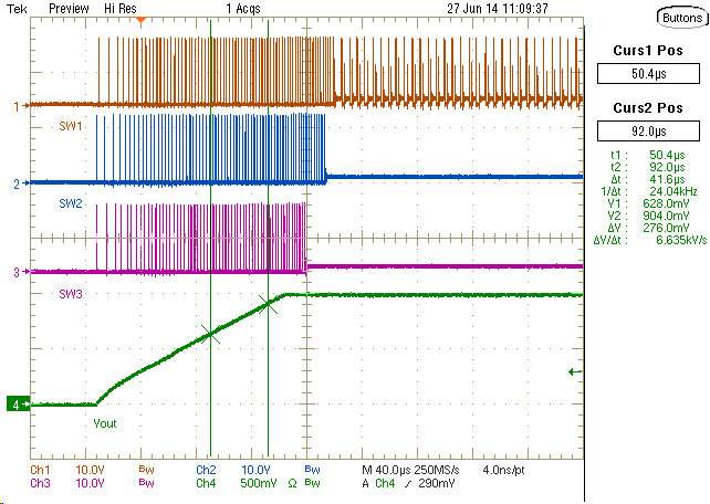
| tSTART-CB | Cold boot time(1) | VBOOT > 0V , EN = high, CREF = 0.33 µF | 1.2 | ms | ||
| tSTBY-E | Standby exit time(3) | VVID = 1.28 V, RSLEW = 39 kΩ | 250 | µs | ||
| SLSET | Slew rate setting for VID change | RSLEW = 20 kΩ | 6 | mV/µs | ||
| RSLEW = 24 kΩ | 12 | |||||
| RSLEW = 30 kΩ | 18 | |||||
| RSLEW = 39 kΩ | 24 | |||||
| RSLEW = 56 kΩ | 30 | |||||
| SLSTART(2) | Slew rate setting for start-up | EN goes high, RSLEW = 39 kΩ | 12 | mV/µs | ||
| ADDR | Address setting 3 LSB of I2C address | VSLEWA ≤ 0.30 V (Addr = 100 0xxx) | 000b | |||
| 0.75 V ≤ VSLEWA ≤ 0.85 V | 011b | |||||
| 1.15 V ≤ VSLEWA ≤ 1.25 V | 101b | |||||
| tPGDDGLTO | PGOOD deglitch time (over)(4) | 1 | µs | |||
| tPGDDGLTU | PGOOD deglitch time (under)(5) | 31 | ||||
| tON | On time | RCF = 20 kΩ | 295 | ns | ||
| RCF = 24 kΩ, VVIN = 12 V, VVFB = 1 V (400 kHz) | 230 | |||||
| RCF = 39 kΩ, VVIN = 12 V, VVFB = 1 V (600 kHz) | 164 | |||||
| RCF = 75 kΩ, VVIN = 12 V, VVFB = 1 V (800 kHz) | 140 | |||||
| RCF = 150 kΩ, VVIN = 12 V, VVFB = 1 V (1 MHz) | 128 | |||||
| PWM AND SKIP OUTPUTS | ||||||
| tP-S_H-L(2) | PWMx/SKIP H-L transition time | 10% to 90%, both edges | 7 | 20 | ns | |
| tP-S_TRI(2) | PWMx tri-state transition | 10% or 90% to tri-state level, both edges | 5 | 20 | ||
| PROTECTION: OVP, UVP, PGOOD AND THERMAL SHUTDOWN | ||||||
| tPG2 | PGOOD low after enable goes low | Low state time after EN goes low. | 225 | 250 | 275 | µs |
(1) Cold boot time is defined as the time from UVLO detection to VOUT ramp.
(2) Specified by design. Not production tested.
(3) Standby exit time is defined as the time from EN assertion until PGOOD goes high
(4) PGOOD deglitch time (over) is defined as the time from when the VFB pin rises above the 250-mV VDAC boundary to when the PGOOD pin goes low.
(5) PGOOD deglitch time (under) is defined as the time from when the VFB pin falls below the –300-mV VDAC boundary to when the PGOOD pin goes low.
6.8 Typical Characteristics (2-Phase Operation)
| VIN = 12 V | VOUT = 1 V | Load = 1 A |
| VIN = 12 V | VOUT = 1 V | Load = 4 A to 20 A |
| VIN = 12 V | VOUT = 1 V | Load = 1 A to 25 A |
| VIN = 12 V | VOUT = 1 V | Load = 10 A |
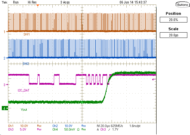
| Δ VOUT, 1.0 V to 1.1 V | I2C command | |
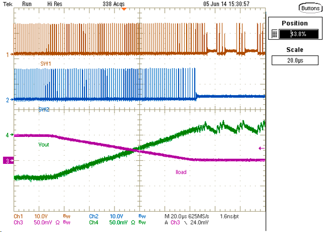
| VIN = 12 V | VOUT = 1 V | Load = 25 A to 1 A |
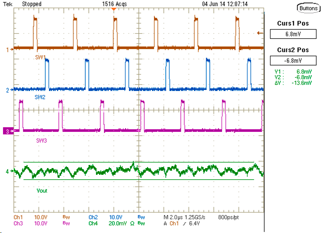
6.9 Typical Characteristics (3-Phase Operation)
| VIN = 12 V | VOUT = 1 V | Load = 1 A |
| VIN = 12 V | VOUT = 1 V | Load = 9 A to 35 A |
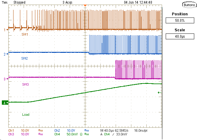
| VIN = 12 V | VOUT = 1 V | Load = 1 A to 31 A |
| VIN = 12 V | VOUT = 1 V | Load = 30 A |
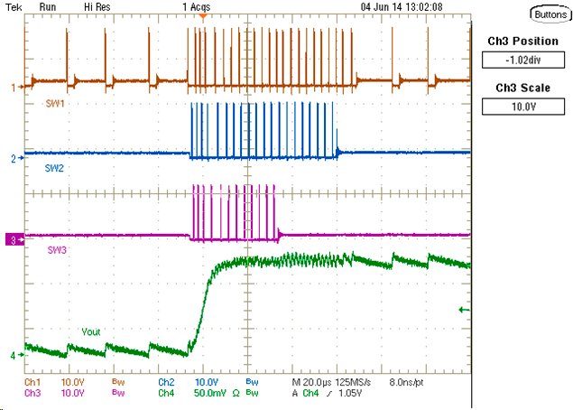
| Δ VOUT, 1.0 V to 1.1 V | I2C command | |
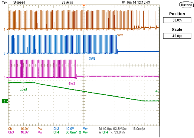
| VIN = 12 V | VOUT = 1 V | Load = 31 A to 1 A |