SLUSBW8 September 2014 TPS53632
PRODUCTION DATA.
- 1 Features
- 2 Applications
- 3 Description
- 4 Revision History
- 5 Pin Configuration and Functions
- 6 Specifications
-
7 Detailed Description
- 7.1 Overview
- 7.2 Functional Block Diagram
- 7.3
Feature Description
- 7.3.1 Current Sensing
- 7.3.2 Load Transients
- 7.3.3 AutoBalance Current Sharing
- 7.3.4 PWM and SKIP Signals
- 7.3.5 5-V, 3.3-V and 1.8-V Undervoltage Lockout (UVLO)
- 7.3.6 Output Undervoltage Protection (UVP)
- 7.3.7 Overcurrent Protection (OCP)
- 7.3.8 Overvoltage Protection
- 7.3.9 Analog Current Monitor, IMON and Corresponding Digital Output Current
- 7.3.10 Addressing
- 7.3.11 I2C Interface Operation
- 7.3.12 Start-Up Sequence
- 7.3.13 Phase Add and Drop Operation
- 7.3.14 Power Good Operation
- 7.3.15 Input Voltage Limits
- 7.3.16 Fault Behavior
- 7.4 Device Functional Modes
- 7.5 Configuration and Programming
- 7.6 Register Maps
-
8 Applications and Implementation
- 8.1
Application Information
- 8.1.1
3-Phase D-CAP+™, Step-Down Application
- 8.1.1.1 Design Requirements
- 8.1.1.2
Detailed Design Procedure
- 8.1.1.2.1 Step 1: Select Switching Frequency
- 8.1.1.2.2 Step 2: Set The Slew Rate
- 8.1.1.2.3 Step 3: Determine Inductor Value And Choose Inductor
- 8.1.1.2.4 Step 4: Determine Current Sensing Method
- 8.1.1.2.5 Step 5: DCR Current Sensing
- 8.1.1.2.6 Step 6: Select OCP Level
- 8.1.1.2.7 Step 7: Set the Load-Line Slope
- 8.1.1.2.8 Step 8: Current Monitor (IMON) Setting
- 8.1.1.3 Application Performance Plots
- 8.1.1.4 Loop Compensation for Zero Load-Line
- 8.1.1
3-Phase D-CAP+™, Step-Down Application
- 8.1
Application Information
- 9 Power Supply Recommendations
- 10 Layout
- 11Device and Documentation Support
- 12Mechanical, Packaging, and Orderable Information
7 Detailed Description
7.1 Overview
The TPS53632 device is a DCAP+ mode adaptive on-time controller. The DAC outputs a reference in accordance with the 8-bit VID code as defined in Table 2. This DAC sets the output voltage.
In adaptive on-time converters, the controller varies the on-time as a function of input and output voltage to maintain a nearly constant frequency during steady-state conditions. With conventional voltage-mode constant on-time converters, each cycle begins when the output voltage crosses to a fixed reference level. However, in the TPS53632 device, the cycle begins when the current feedback reaches an error voltage level which corresponds to the amplified difference between the DAC voltage and the feedback output voltage. In the case of two-phase or three-phase operation, the device sums the current feedback from all the phases at the output of the internal current-sense amplifiers.
This approach has two advantages:
- The amplifier DC gain sets an accurate linear load-line slope, which is required for CPU core applications.
- The device filters the error voltage input to the PWM comparator to improve the noise performance.
In addition, a value representing the difference between the DAC-to-output voltage and the current feedback, goes through an integrator to give an approximately linear load-line slope even at light loads where the inductor current is in discontinuous conduction mode (DCM).
During a steady-state condition, the phases of the TPS53632 switch 180° phase-displacement for two-phase mode and 120° phase-displacement for three-phase mode. The phase displacement is maintained both by the architecture (which does not allow the high-side gate drive outputs of more than one phase to be ON in any condition except transients) and the current ripple (which forces the pulses to be spaced equally). The controller forces current-sharing by adjusting the ON-time of each phase. Current balancing requires no user intervention, compensation, or extra components.
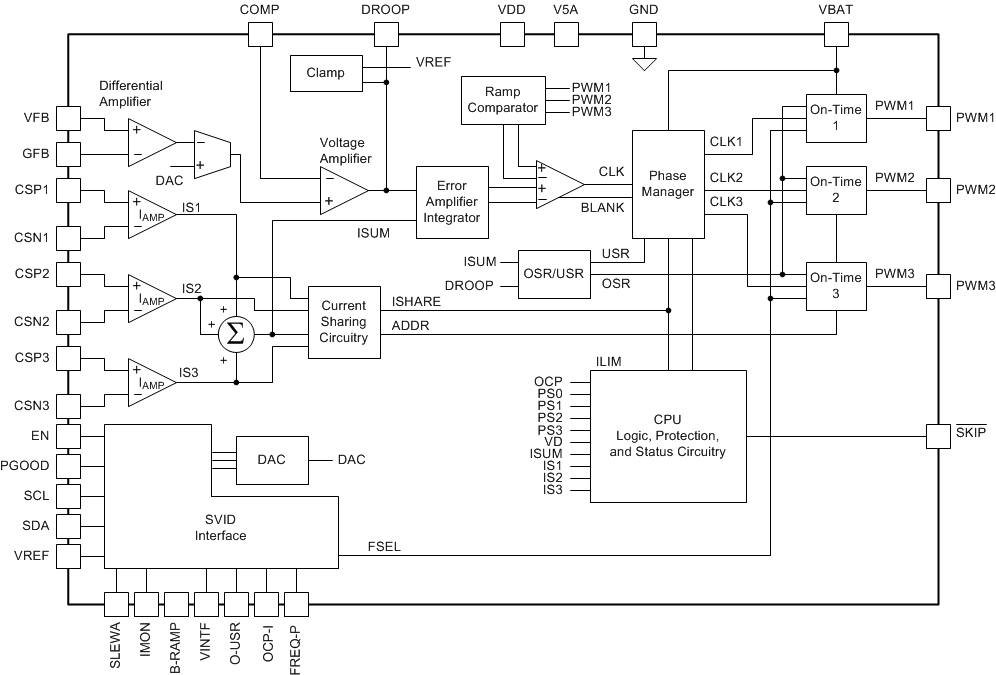
7.2 Functional Block Diagram
7.3 Feature Description
7.3.1 Current Sensing
The TPS53632 device provides independent channels of current feedback for every phase. These independent channels increase the system accuracy and reduce the dependence of circuit performance on layout compared to an externally summed architecture. The design can use inductor DCR sensing to yield the best efficiency or resistor current sensing to yield the most accuracy across wide temperature ranges. DCR sensing can be optimized by using a NTC thermistor to reduce the variation of current sense with temperature.
The pins CSP1, CSN1, CSP2, CSN2 and CSP3, CSN3 are the current sensing pins.
7.3.2 Load Transients
When the load increases suddenly, the output voltage immediately drops. This voltage drop is reflected as a rising voltage on the DROOP pin. This rising voltage forces the PWM to pulse sooner and more frequently which causes the inductor current to rapidly increase. As the inductor current reaches the new load current, a steady-state operating condition is reached and the PWM switching resumes the steady-state frequency. Similarly, when the load releases suddenly, the output voltage rises. This rise is reflected as a falling voltage on the COMP pin. This rising voltage forces a delay in the PWM pulses until the inductor current reaches the new load current, when the switching resumes and steady-state switching continues.
7.3.3 AutoBalance™ Current Sharing
The basic mechanism for current sharing is to sense the average phase current, then adjust the pulse width of each phase to equalize the current in each phase.
The PWM comparator (not shown) starts a pulse when the feedback voltage equals the reference voltage. The VIN voltage charges the Ct(on) capacitor through the resistor Rt(on). The pulse is terminated when the voltage at capacitor Ct(on) matches the on-time (tON) reference, normally the DAC voltage (VDAC).
A current sharing circuit is shown in Figure 13. For example, assume that the 5 µs averaged value of I1 = I2 = I3. In this case, the PWM modulator terminates at VDAC, and the normal pulse width is delivered to the system. If instead, I1 > IAVG, then an offset is subtracted from VDAC, and the pulse width for Phase 1 is shortened, reducing the current in Phase 1 to compensate. If I1 < IAVG, then a longer pulse is produced, again compensating on a pulse-by-pulse basis.
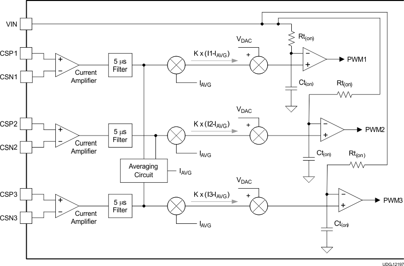 Figure 13. AutoBalance Current Sharing
7.3.4 PWM and SKIP Signals
The PWM and SKIP signals are outputs of the controller and serve as input to the driver or DrMOS type devices. Both are 5-V logic signals. The PWM signals are logic high when the high-side driver turns ON. The PWM signal must be low for the low-side drive to turn ON. When both the drive signals are OFF, the PWM is in tri-state.
7.3.5 5-V, 3.3-V and 1.8-V Undervoltage Lockout (UVLO)
The TPS53632 device continuously monitors the voltage on the V5A, VDD and VINTF pins to ensure a value high enough to bias the device properly and provide sufficient gate drive potential to maintain high efficiency. The converter starts with a voltage of approximately 4.4 V and has a nominal 200 mV of hysteresis. After the 5VA, VDD or VINTF pins go below the VUVLOL level, the corresponding voltage must fall below VPOR (1.5 V) to reset the device.
The input voltage (VVIN) does not include a UVLO function, so the circuit runs with power inputs as low as approximately 3 x VOUT.
7.3.6 Output Undervoltage Protection (UVP)
Output undervoltage protection works in conjunction with the current protection described in the Overcurrent Protection (OCP) section. If the output voltage drops below the low PGOOD voltage threshold, then the drivers are turned OFF until the EN pin power is cycled.
7.3.7 Overcurrent Protection (OCP)
The TPS53632 device uses a valley current limiting scheme, so the ripple current must be considered. The DC current value at OCP (IOCP) is the OCP limit value plus half of the ripple current. Current limiting occurs on a phase-by-phase and pulse-by-pulse basis. If the voltage between the CSPx and CSNx pins is above the OCP value, the converter delays the next ON pulse until that voltage difference drops below the OCP limit. For inductor current sensing circuits, the voltage between the CSPx and CSNx pins is the inductor DCR value multiplied by the resistor divider which is part of the NTC compensation network. As a result, a wide range of OCP values can be obtained by changing the resistor divider value. In general, use the highest OCP setting possible with the least attenuation in the resistor divider to provide as much signal to the device as possible. This provides the best performance for all parameters related to current feedback.
In OCP mode, the voltage drops until the UVP limit is reached. Then the converter sets the PGOOD to inactive, and the drivers are turned OFF. The converter remains in this state until the device is reset by the V5A, VDD or VINTF rails.
7.3.8 Overvoltage Protection
An OVP condition is detected when the output voltage is greater than the PGDH voltage, and greater than VDAC. VOUT > + VPGDH greater than VDAC. In this case, the converter sets PGOOD inactive, and turns ON the drive for the low-side MOSFET. The converter remains in this state until the device is reset by cycling the V5A, VDD or VINTF pin. However, the OVP threshold is blanked much of the time. In order to provide protection to the processor 100% of the time, there is a second OVP level fixed at VOVPH which is always active. If the fixed OVP condition is detected, the PGOOD are forced inactive and the low-side MOSFETs are tuned ON. The converter remains in this state until the V5A, VDD or VINTF pin is reset.
7.3.9 Analog Current Monitor, IMON and Corresponding Digital Output Current
The TPS53632 device includes a current monitor function. The current monitor supplies an analog voltage, proportional to the load current, on the IMON pin.
The current monitor function is related to the OCP selection resistors. The ROCP is the resistor between the OCP-I pin and GND and RCIMON is the resistor between the IMON pin to the OCP-I pin that sets the current monitor gain. Equation 1 shows the calculation for the current monitor gain.
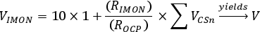
where
- Σ VCS is the sum of the DC voltages at the inputs to the current sense amplifiers
To ensure stable current monitor operation and at the same time provide a fast dynamic response, connect a capacitor with a value between 4.7-nF and 10-nF between the IMON pin and GND.
Set the analog current monitor so that at the maximum processor current (ICC(max)) level, the IMON voltage is 1.7 V. This corresponds to a digital output current value of ‘FF’ in register 03H.
7.3.10 Addressing
The TPS53632 device can be configured for three different base addresses by setting a voltage on the SLEWA pin. Configure a resistor divider on SLEWA from VREF to GND. A resistor between the SLEWA pin and GND sets the slew rate. Once the slew rate resistor is selected, the resistor from the VREF pin to the SLEWA pin can be chosen based on the required base address. For a base address of 0, the VREF to SLEWA resistor can be left open.
7.3.11 I2C Interface Operation
The TPS53632 device includes a slave I2C interface accessed via the SCL (serial clock) and SDA (serial data) pins. The interface sets the base VID value, receives current monitor telemetry, and controls functions described in this section. It operates when EN = low, with the bias supplies in regulation. It is compliant with I2C specification UM10204, Revision 3.0. The characteristics are:
- Addressing
- 7-bit addressing; address range is 100 0xxx (binary)
- Last three bits are determined by the SLEWA pin at start-up
- Byte read / byte write protocols only (See figures below)
- Frequency
- 100 kHz
- 400 kHz
- 1 MHz
- 3.4 MHz
- Logic inputs are 1.8-V logic levels (3.3-V tolerant)
7.3.11.1 Key for Protocol Examples
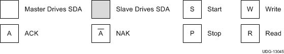
7.3.11.2 Protocol Examples
The good byte read transaction the controller ACKs and the master terminates with a NAK/stop.
 Figure 14. Good Byte Read Transaction
The controller issues a NAK to the read command with an invalid register address.
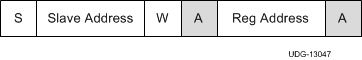 Figure 15. NAK Invalid Register Address
Figure 16 illustrates a good byte write.
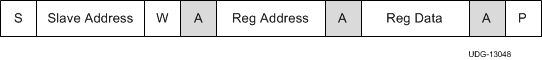 Figure 16. Good Byte Write
The controller issues a NAK to a write command with an invalid register address.
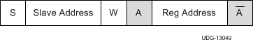 Figure 17. Invalid NAK Register Address
The controller issues a NAK to a write command for the condition of invalid data.
 Figure 18. Invalid NAK Register Data
The following master code sequence is executed to enter Hs (3.4-MHz SCL) mode.
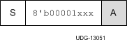 Figure 19. Master Code Sequence
7.3.12 Start-Up Sequence
The TPS53632 initializes when all of the supply voltages rise above the UVLO thresholds. This function is also know as a cold boot. The device then reads all of the various settings (such as frequency and overcurrent protection). This process takes less than 1.2 ms. During this time, the VSR pin initializes to the BOOT voltage. The output voltage rises to the voltage select register (VSR) level when the EN pin (enable) goes high. As soon as the BOOT sequence completes, PGOOD is HIGH and the I2C interface can be used to change the voltage select register. The current VSR value is held when EN goes low and returns to a high state This function is also know as a warm boot). The VSR can be changed when EN is low, however, this is not recommended prior to completion of the cold boot process.
7.3.13 Phase Add and Drop Operation
The phase add and phase drop operations are enabled by default in the TPS53632 device. The converter starts up in multi-phase CCM mode and reduces phase count until reaching single phase DCM mode as the load is reduced. This action takes place at a fixed percentage of the OCP level defined in the Electrical Characteristics table. The controller automatically adds phases when the current exceeds the defined percentage of the OCP value.
To disable the automatic phase and drop operation, connect a resistor between the VREF pin and the FREQ-P pin so that the voltage is above the value specified in the parameter table.
7.3.14 Power Good Operation
PGOOD is an open-drain output pin that is designed to be pulled up with an external resistor to a voltage 3.6 V or less. Normal PGOOD operation (exclusive of OC or MAXVID interrupt action) is shown in Figure 20. On initial power-up, a power good status occurs within 6 µs of the DAC reaching its target value. When EN is brought low, the PGOOD pin is also brought low for 250 µs and then is allowed to float. The TPS53632 device pulls down the PGOOD signal when the EN signal subsequently goes high and returns high again within 6 µs of the end of the DAC ramp. The delay period between the EN pin going high and the PGOOD pin going low in this case is less than 1 µs.
Figure 20 shows the power good operation at initial start up and with falling and rising EN.
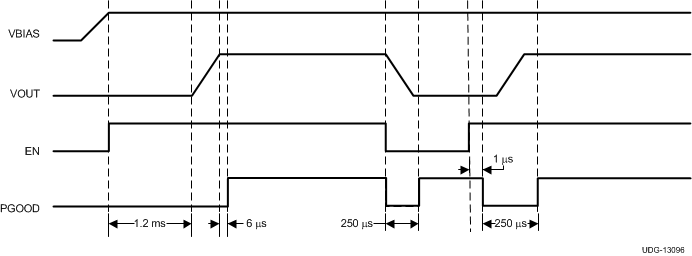 Figure 20. Power Good Operation
7.3.15 Input Voltage Limits
The number of input phases supported varies with the input voltage. See Table 1 for limits. The minimum input voltage is lower for lower frequency operation and/or lower output voltages.
Table 1. Input Voltage Limits vs Number of Phases at 1-MHz Switching Frequency
| NUMBER OF PHASES | VIN(min) (V) | VOUT(max) (V) |
|---|---|---|
| 3 | 5.5 | 1.28 |
| 2 | 3.7 | |
| 1 | 2.5 |
7.3.16 Fault Behavior
The TPS53632 device has a complete suite of fault detection and protection functions, including input undervoltage lockout (UVLO) on all power inputs, overvoltage and overcurrent limiting and output undervoltage detection. The protection limits are summarized in Table 1. The converter suspends switching when the limits are exceeded and the PGOOD pin goes low. In this state, the fault register 14h is readable. To exit fault protection mode, power must be cycled.
Table 2. TPS53632 VID Table
| VID6 | VID5 | VID4 | VID3 | VID2 | VID1 | VID0 | HEX | VOLTAGE |
|---|---|---|---|---|---|---|---|---|
| 0 | 0 | 1 | 1 | 0 | 0 | 1 | 19 | 0.5000 |
| 0 | 0 | 1 | 1 | 0 | 1 | 0 | 1A | 0.5100 |
| 0 | 0 | 1 | 1 | 0 | 1 | 1 | 1B | 0.5200 |
| 0 | 0 | 1 | 1 | 1 | 0 | 0 | 1C | 0.5300 |
| 0 | 0 | 1 | 1 | 1 | 0 | 1 | 1D | 0.5400 |
| 0 | 0 | 1 | 1 | 1 | 1 | 0 | 1E | 0.5500 |
| 0 | 0 | 1 | 1 | 1 | 1 | 1 | 1F | 0.5600 |
| 0 | 1 | 0 | 0 | 0 | 0 | 0 | 20 | 0.5700 |
| 0 | 1 | 0 | 0 | 0 | 0 | 1 | 21 | 0.5800 |
| 0 | 1 | 0 | 0 | 0 | 1 | 0 | 22 | 0.5900 |
| 0 | 1 | 0 | 0 | 0 | 1 | 1 | 23 | 0.6000 |
| 0 | 1 | 0 | 0 | 1 | 0 | 0 | 24 | 0.6100 |
| 0 | 1 | 0 | 0 | 1 | 0 | 1 | 25 | 0.6200 |
| 0 | 1 | 0 | 0 | 1 | 1 | 0 | 26 | 0.6300 |
| 0 | 1 | 0 | 0 | 1 | 1 | 1 | 27 | 0.6400 |
| 0 | 1 | 0 | 1 | 0 | 0 | 0 | 28 | 0.6500 |
| 0 | 1 | 0 | 1 | 0 | 0 | 1 | 29 | 0.6600 |
| 0 | 1 | 0 | 1 | 0 | 1 | 0 | 2A | 0.6700 |
| 0 | 1 | 0 | 1 | 0 | 1 | 1 | 2B | 0.6800 |
| 0 | 1 | 0 | 1 | 1 | 0 | 0 | 2C | 0.6900 |
| 0 | 1 | 0 | 1 | 1 | 0 | 1 | 2D | 0.7000 |
| 0 | 1 | 0 | 1 | 1 | 1 | 0 | 2E | 0.7100 |
| 0 | 1 | 0 | 1 | 1 | 1 | 1 | 2F | 0.7200 |
| 0 | 1 | 1 | 0 | 0 | 0 | 0 | 30 | 0.7300 |
| 0 | 1 | 1 | 0 | 0 | 0 | 1 | 31 | 0.7400 |
| 0 | 1 | 1 | 0 | 0 | 1 | 0 | 32 | 0.7500 |
| 0 | 1 | 1 | 0 | 0 | 1 | 1 | 33 | 0.7600 |
| 0 | 1 | 1 | 0 | 1 | 0 | 0 | 34 | 0.7700 |
| 0 | 1 | 1 | 0 | 1 | 0 | 1 | 35 | 0.7800 |
| 0 | 1 | 1 | 0 | 1 | 1 | 0 | 36 | 0.7900 |
| 0 | 1 | 1 | 0 | 1 | 1 | 1 | 37 | 0.8000 |
| 0 | 1 | 1 | 1 | 0 | 0 | 0 | 38 | 0.8100 |
| 0 | 1 | 1 | 1 | 0 | 0 | 1 | 39 | 0.8200 |
| 0 | 1 | 1 | 1 | 0 | 1 | 0 | 3A | 0.8300 |
| 0 | 1 | 1 | 1 | 0 | 1 | 1 | 3B | 0.8400 |
| 0 | 1 | 1 | 1 | 1 | 0 | 0 | 3C | 0.8500 |
| 0 | 1 | 1 | 1 | 1 | 0 | 1 | 3D | 0.8600 |
| 0 | 1 | 1 | 1 | 1 | 1 | 0 | 3E | 0.8700 |
| 0 | 1 | 1 | 1 | 1 | 1 | 1 | 3F | 0.8800 |
| 1 | 0 | 0 | 0 | 0 | 0 | 0 | 40 | 0.8900 |
| 1 | 0 | 0 | 0 | 0 | 0 | 1 | 41 | 0.9000 |
| 1 | 0 | 0 | 0 | 0 | 1 | 0 | 42 | 0.9100 |
| 1 | 0 | 0 | 0 | 0 | 1 | 1 | 43 | 0.9200 |
| 1 | 0 | 0 | 0 | 1 | 0 | 0 | 44 | 0.9300 |
| 1 | 0 | 0 | 0 | 1 | 0 | 1 | 45 | 0.9400 |
| 1 | 0 | 0 | 0 | 1 | 1 | 0 | 46 | 0.9500 |
| 1 | 0 | 0 | 0 | 1 | 1 | 1 | 47 | 0.9600 |
| 1 | 0 | 0 | 1 | 0 | 0 | 0 | 48 | 0.9700 |
| 1 | 0 | 0 | 1 | 0 | 0 | 1 | 49 | 0.9800 |
| 1 | 0 | 0 | 1 | 0 | 1 | 0 | 4A | 0.9900 |
| 1 | 0 | 0 | 1 | 0 | 1 | 1 | 4B | 1.0000 |
| 1 | 0 | 0 | 1 | 1 | 0 | 0 | 4C | 1.0100 |
| 1 | 0 | 0 | 1 | 1 | 0 | 1 | 4D | 1.0200 |
| 1 | 0 | 0 | 1 | 1 | 1 | 0 | 4E | 1.0300 |
| 1 | 0 | 0 | 1 | 1 | 1 | 1 | 4F | 1.0400 |
| 1 | 0 | 1 | 0 | 0 | 0 | 0 | 50 | 1.0500 |
| 1 | 0 | 1 | 0 | 0 | 0 | 1 | 51 | 1.0600 |
| 1 | 0 | 1 | 0 | 0 | 1 | 0 | 52 | 1.0700 |
| 1 | 0 | 1 | 0 | 0 | 1 | 1 | 53 | 1.0800 |
| 1 | 0 | 1 | 0 | 1 | 0 | 0 | 54 | 1.0900 |
| 1 | 0 | 1 | 0 | 1 | 0 | 1 | 55 | 1.1000 |
| 1 | 0 | 1 | 0 | 1 | 1 | 0 | 56 | 1.1100 |
| 1 | 0 | 1 | 0 | 1 | 1 | 1 | 57 | 1.1200 |
| 1 | 0 | 1 | 1 | 0 | 0 | 0 | 58 | 1.1300 |
| 1 | 0 | 1 | 1 | 0 | 0 | 1 | 59 | 1.1400 |
| 1 | 0 | 1 | 1 | 0 | 1 | 0 | 5A | 1.1500 |
| 1 | 0 | 1 | 1 | 0 | 1 | 1 | 5B | 1.1600 |
| 1 | 0 | 1 | 1 | 1 | 0 | 0 | 5C | 1.1700 |
| 1 | 0 | 1 | 1 | 1 | 0 | 1 | 5D | 1.1800 |
| 1 | 0 | 1 | 1 | 1 | 1 | 0 | 5E | 1.1900 |
| 1 | 0 | 1 | 1 | 1 | 1 | 1 | 5F | 1.2000 |
| 1 | 1 | 0 | 0 | 0 | 0 | 0 | 60 | 1.2100 |
| 1 | 1 | 0 | 0 | 0 | 0 | 1 | 61 | 1.2200 |
| 1 | 1 | 0 | 0 | 0 | 1 | 0 | 62 | 1.2300 |
| 1 | 1 | 0 | 0 | 0 | 1 | 1 | 63 | 1.2400 |
| 1 | 1 | 0 | 0 | 1 | 0 | 0 | 64 | 1.2500 |
| 1 | 1 | 0 | 0 | 1 | 0 | 1 | 65 | 1.2600 |
| 1 | 1 | 0 | 0 | 1 | 1 | 0 | 66 | 1.2700 |
| 1 | 1 | 0 | 0 | 1 | 1 | 1 | 67 | 1.2800 |
| 1 | 1 | 0 | 1 | 0 | 0 | 0 | 68 | 1.2900 |
| 1 | 1 | 0 | 1 | 0 | 0 | 1 | 69 | 1.3000 |
| 1 | 1 | 0 | 1 | 0 | 1 | 0 | 6A | 1.3100 |
| 1 | 1 | 0 | 1 | 0 | 1 | 1 | 6B | 1.3200 |
| 1 | 1 | 0 | 1 | 1 | 0 | 0 | 6C | 1.3300 |
| 1 | 1 | 0 | 1 | 1 | 0 | 1 | 6D | 1.3400 |
| 1 | 1 | 0 | 1 | 1 | 1 | 0 | 6E | 1.3500 |
| 1 | 1 | 0 | 1 | 1 | 1 | 1 | 6F | 1.3600 |
| 1 | 1 | 1 | 0 | 0 | 0 | 0 | 70 | 1.3700 |
| 1 | 1 | 1 | 0 | 0 | 0 | 1 | 71 | 1.3800 |
| 1 | 1 | 1 | 0 | 0 | 1 | 0 | 72 | 1.3900 |
| 1 | 1 | 1 | 0 | 0 | 1 | 1 | 73 | 1.4000 |
| 1 | 1 | 1 | 0 | 1 | 0 | 0 | 74 | 1.4100 |
| 1 | 1 | 1 | 0 | 1 | 0 | 1 | 75 | 1.4200 |
| 1 | 1 | 1 | 0 | 1 | 1 | 0 | 76 | 1.4300 |
| 1 | 1 | 1 | 0 | 1 | 1 | 1 | 77 | 1.4400 |
| 1 | 1 | 1 | 1 | 0 | 0 | 0 | 78 | 1.4500 |
| 1 | 1 | 1 | 1 | 0 | 0 | 1 | 79 | 1.4600 |
| 1 | 1 | 1 | 1 | 0 | 1 | 0 | 7A | 1.4700 |
| 1 | 1 | 1 | 1 | 0 | 1 | 1 | 7B | 1.4800 |
| 1 | 1 | 1 | 1 | 1 | 0 | 0 | 7C | 1.4900 |
| 1 | 1 | 1 | 1 | 1 | 0 | 1 | 7D | 1.5000 |
| 1 | 1 | 1 | 1 | 1 | 1 | 0 | 7E | 1.5100 |
| 1 | 1 | 1 | 1 | 1 | 1 | 1 | 7F | 1.5200 |
7.4 Device Functional Modes
7.4.1 PWM Operation
The Functional Block Diagram and Figure 21 show how the converter operates in continuous conduction mode (CCM).
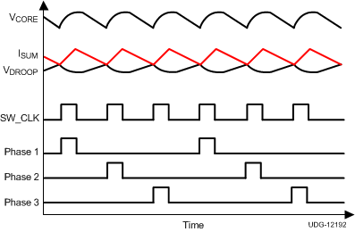 Figure 21. D-CAP+™ Mode Basic Waveforms
Starting with the condition that the high-side FETs are off and the low-side FETs are on, the summed current feedback (ISUM) is higher than the error amplifier output (VCOMP). ICMP falls until it hits VCOMP, which contains a component of the output ripple voltage. The PWM comparator senses where the two waveforms cross and triggers the on-time generator, which generates the internal SW_CLK signal. Each SW_CLK signal corresponds to one switching ON pulse for one phase.
During single-phase operation, every SW_CLK signal generates a switching pulse on the same phase. Also, ISUM voltage corresponds to a single-phase inductor current only.
During multi-phase operation, the controller distributes the SW_CLK signal to each of the phases in a cycle. Using the summed inductor current and cyclically distributing the ON pulses to each phase automatically gives the required interleaving of 360/n, where n is the number of phases.
7.5 Configuration and Programming
After the 5-V, 3.3-V, or VINTF power is applied to the controller (all are above UVLO level), the following information is latched and cannot be changed anytime during operation. The Electrical Characteristics table defines the values of the selections.
7.5.1 Operating Frequency
The resistor between the FREQ-P pin and GND sets the switching frequency. See the Electrical Characteristics table for the resistor settings corresponding to each frequency selection.
NOTE
The operating frequency is a quasi-fixed frequency in the sense that the ON time is fixed based on the input voltage (at the VIN pin) and output voltage (set by VID). The OFF time varies based on various factors such as load and power-stage components.
7.5.2 Overcurrent Protection (OCP) Level
The resistor from OCP-I to GND sets the OCP level of the CPU channel. See the Electrical Characteristics table for the resistor settings corresponding to each OCP level.
7.5.3 IMON Gain
The resistors from IMON to OCP-I and OCP-I to GND set the DC load current monitor (IMON) gain.
7.5.4 Slew Rate
The SetVID fast slew rate is set by the resistor from SLEWA pin to GND. See the Electrical Characteristics table for the resistor settings corresponding to each slew rate setting.
7.5.5 Base Address
The voltage on SLEWA pin sets the device base address.
7.5.6 Ramp Selection
The resistor from RAMP to GND sets the ramp compensation level. See the Electrical Characteristics table for the resistor settings corresponding to each ramp level.
7.5.7 Active Phases
Normally, the controller is configured to operate in 3-phase mode. To enable 2-phase mode, tie the CSP3 pin to a 3.3-V supply and the CSN3 pin to GND. To enable 1-phase mode, tie the CSP2 and CSP3 pins to a 3.3-V supply and tie the CSN2 and CSN3 pins to GND.
7.6 Register Maps
The I2C interface can support 400-kHz, 1-MHz, and 3.4-MHz clock frequencies. The I2C interface is accessible even when EN is low. The following registers are accessible via I2C.
7.6.1 Voltage Select Register (VSR) (00h)
- Type: Read and write
- Power-up value: 48h. This value can be changed before the rising edge of EN to change BOOT voltage.
- EN rising (after power-up): prior programmed value
- See Table 2 for exact values
- A command to set VSR < 19h (minimum VID) generates a NAK and the VSR remains at the prior value
| b7 | b6 | b5 | b4 | b3 | b2 | b1 | b0 |
|---|---|---|---|---|---|---|---|
| – | VID[6:0] | ||||||
7.6.2 IMON Register (03h)
- Type: Read only
- Power-up value: 00h
- EN rising (after power-up):00h
| b7 | b6 | b5 | b4 | b3 | b2 | b1 | b0 |
|---|---|---|---|---|---|---|---|
| MSB | – | – | – | – | – | – | LSB |
7.6.3 VMAX Register (04h)
- Type: Read / write (see below)
- Power-up value: 1.28 V (OTP value)
- EN rising (after power-up): Last written value
| b7 | b6 | b5 | b4 | b3 | b2 | b1 | b0 |
|---|---|---|---|---|---|---|---|
| Lock | MSB | – | – | – | – | – | LSB |
Bit definitions:
| BIT | NAME | DEFINITION |
|---|---|---|
| 0 - 6 | VMAX | Maximum VID setting |
| 7 | Lock | Access protection of the VMAX register 0: No protection, R/W access to bits 0-6 1: Access is read only; reset after UVLO event. |
7.6.4 Power State Register (06h)
- Type: Read and write
- Power-up value: 00h
- EN rising (after power-up): 00h
| b7 | b6 | b5 | b4 | b3 | b2 | b1 | b0 |
|---|---|---|---|---|---|---|---|
| – | – | – | – | – | – | MSB | LSB |
Bit definitions:
| VALUE | DEFINITION |
|---|---|
| 0 | Multi-phase CCM |
| 1 | Single-phase CCM |
| 2 | Single-phase DCM |
7.6.5 SLEW Register (07h)
- Type: Read and write (see below)
- Power-up value: Defined by SLEWA pin at power-up
- EN rising (after power-up): Last written value
- Write only a single ‘1’ for the SLEW rate desired
| b7 | b6 | b5 | b4 | b3 | b2 | b1 | b0 |
|---|---|---|---|---|---|---|---|
| 48 mV/µs | 42mV/µs | 36 mV/µs | 30 mV/µs | 24 mV/µs | 18 mV/µs | 12 mV/µs | 6 mV/µs |
7.6.6 Lot Code Registers (10-13h)
- Type: 8-bits; read only
- Power-up value: Programmed at factory
7.6.7 Fault Register (14h)
- Type: 8-bits; read only
- Power-up value: 00h
| b7 | b6 | b5 | b4 | b3 | b2 | b1 | b0 |
|---|---|---|---|---|---|---|---|
| – | – | – | – | Device thermal shutdown | OVP | UVP | OCP |