JAJSOW5F April 2006 – January 2024 TPS5420
PRODUCTION DATA
- 1
- 1特長
- 2アプリケーション
- 3概要
- 4静電気放電に関する注意事項
- 5Ordering Information
- 6Pin Assignments
- 7Specifications
-
8Application Information
- 8.1 Functional Block Diagram
- 8.2
Detailed Description
- 8.2.1 Oscillator Frequency
- 8.2.2 Voltage Reference
- 8.2.3 Enable (ENA) and Internal Slow Start
- 8.2.4 Undervoltage Lockout (UVLO)
- 8.2.5 Boost Capacitor (BOOT)
- 8.2.6 Output Feedback (VSENSE)
- 8.2.7 Internal Compensation
- 8.2.8 Voltage Feed Forward
- 8.2.9 Pulse-Width-Modulation (PWM) Control
- 8.2.10 Overcurrent Limiting
- 8.2.11 Overvoltage Protection
- 8.2.12 Thermal Shutdown
- 8.2.13 PCB Layout
- 8.2.14 Application Circuits
- 8.2.15
Design Procedure
- 8.2.15.1 Design Parameters
- 8.2.15.2 Switching Frequency
- 8.2.15.3 Input Capacitors
- 8.2.15.4 Output Filter Components
- 8.2.15.5 Output Voltage Setpoint
- 8.2.15.6 Boot Capacitor
- 8.2.15.7 Catch Diode
- 8.2.15.8 Additional Circuits
- 8.2.15.9 Circuit Using Ceramic Output Filter Capacitors
- 8.2.15.10 Output Filter Component Selection
- 8.2.15.11 External Compensation Network
- 8.3 Advanced Information
- 8.4 Performance Graphs
- 9Revision History
8.2.15.3 Input Capacitors
The TPS5420 requires an input decoupling capacitor and, depending on the application, a bulk input capacitor. The recommended value for the decoupling capacitor is 10 μF. A high quality ceramic type X5R or X7R is required. For some applications, a smaller value decoupling capacitor may be used, if the input voltage and current ripple ratings are not exceeded. The voltage rating must be greater than the maximum input voltage, including ripple. For this design, two 4.7 μF capacitors, C1 and C4 are used to allow for smaller 1812 case size to be used while maintaining a 50 V rating.
This input ripple voltage can be approximated by Equation 2 :
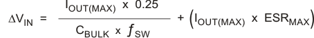
Where IOUT(MAX) is the maximum load current, fSW is the switching frequency, CI is the input capacitor value and ESRMAX is the maximum series resistance of the input capacitor.
The maximum RMS ripple current also needs to be checked. For worst case conditions, this is approximated by Equation 3:

In this example, the calculated input ripple voltage is 118 mV, and the RMS ripple current is 1.0 A. The maximum voltage across the input capacitors would be VIN max plus delta VIN/2. The chosen input decoupling capacitors are rated for 50 V, and the ripple current capacity for each is 3 A at 500 kHz, providing ample margin. The actual measured input ripple voltage may be larger than the calculated value due to the output impedance of the input voltage source and parasitics associated with the layout.
The maximum ratings for voltage and current are not to be exceeded under any circumstance.
Additionally, some bulk capacitance may be needed, especially if the TPS5420 circuit is not located within approximately 2 inches from the input voltage source. The value for this capacitor is not critical but it should be rated to handle the maximum input voltage including ripple voltage and should filter the output so that input ripple voltage is acceptable.