JAJSOW5F April 2006 – January 2024 TPS5420
PRODUCTION DATA
- 1
- 1特長
- 2アプリケーション
- 3概要
- 4静電気放電に関する注意事項
- 5Ordering Information
- 6Pin Assignments
- 7Specifications
-
8Application Information
- 8.1 Functional Block Diagram
- 8.2
Detailed Description
- 8.2.1 Oscillator Frequency
- 8.2.2 Voltage Reference
- 8.2.3 Enable (ENA) and Internal Slow Start
- 8.2.4 Undervoltage Lockout (UVLO)
- 8.2.5 Boost Capacitor (BOOT)
- 8.2.6 Output Feedback (VSENSE)
- 8.2.7 Internal Compensation
- 8.2.8 Voltage Feed Forward
- 8.2.9 Pulse-Width-Modulation (PWM) Control
- 8.2.10 Overcurrent Limiting
- 8.2.11 Overvoltage Protection
- 8.2.12 Thermal Shutdown
- 8.2.13 PCB Layout
- 8.2.14 Application Circuits
- 8.2.15
Design Procedure
- 8.2.15.1 Design Parameters
- 8.2.15.2 Switching Frequency
- 8.2.15.3 Input Capacitors
- 8.2.15.4 Output Filter Components
- 8.2.15.5 Output Voltage Setpoint
- 8.2.15.6 Boot Capacitor
- 8.2.15.7 Catch Diode
- 8.2.15.8 Additional Circuits
- 8.2.15.9 Circuit Using Ceramic Output Filter Capacitors
- 8.2.15.10 Output Filter Component Selection
- 8.2.15.11 External Compensation Network
- 8.3 Advanced Information
- 8.4 Performance Graphs
- 9Revision History
8.2.15.10 Output Filter Component Selection
Using Equation 11, the minimum inductor value is 17.9 μH. A value of 18 μH is chosen for this design.
When using ceramic output filer capacitors, the recommended LC resonant frequency should be no more than 7 kHz. Since the output inductor is already selected at 18 μH, this limits the minimum output capacitor value to:
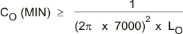
The minimum capacitor value is calculated to be 29 μF. For this circuit a larger value of capacitor yields better transient response. Two 47 μF output capacitors are used for C3 and C4. It is important to note that the actual capacitance of ceramic capacitors decreases with applied voltage. In this example, the output voltage is set to 3.3 V, minimizing this effect.