JAJSBO6B June 2012 – May 2019 TPS54678
PRODUCTION DATA.
- 1 特長
- 2 アプリケーション
- 3 概要
- 4 改訂履歴
- 5 概要(続き)
- 6 Pin Configuration and Functions
- 7 Specifications
-
8 Detailed Description
- 8.1 Overview
- 8.2 Functional Block Diagram
- 8.3
Feature Description
- 8.3.1 Fixed Frequency PWM Control
- 8.3.2 Slope Compensation and Output Current
- 8.3.3 Bootstrap Voltage (Boot) and Low Dropout Operation
- 8.3.4 Error Amplifier
- 8.3.5 Voltage Reference
- 8.3.6 Adjusting the Output Voltage
- 8.3.7 Enable and Adjusting Undervoltage Lockout
- 8.3.8 Soft-Start Pin
- 8.3.9 Sequencing
- 8.3.10 Constant Switching Frequency and Timing Resistor (RT/CLK Pin)
- 8.3.11 Overcurrent Protection
- 8.3.12 Safe Start-Up into Prebiased Outputs
- 8.3.13 Synchronize Using the RT/CLK Pin
- 8.3.14 Power Good (PWRGD Pin)
- 8.3.15 Overvoltage Transient Protection
- 8.3.16 Thermal Shutdown
- 8.4 Device Functional Modes
-
9 Application and Implementation
- 9.1 Application Information
- 9.2
Typical Application
- 9.2.1 Design Requirements
- 9.2.2
Detailed Design Procedure
- 9.2.2.1 Custom Design With WEBENCH® Tools
- 9.2.2.2 Step One: Select the Switching Frequency
- 9.2.2.3 Step Two: Select the Output Inductor
- 9.2.2.4 Step Three: Choose the Output Capacitor
- 9.2.2.5 Step Four: Select the Input Capacitor
- 9.2.2.6 Step Five: Choose the Soft-Start Capacitor
- 9.2.2.7 Step Six: Select the Bootstrap Capacitor
- 9.2.2.8 Step Eight: Select Output Voltage and Feedback Resistors
- 9.2.2.9 Step Nine: Select Loop Compensation Components
- 9.2.3 Application Curves
- 10Power Supply Recommendations
- 11Layout
- 12デバイスおよびドキュメントのサポート
- 13メカニカル、パッケージ、および注文情報
パッケージ・オプション
メカニカル・データ(パッケージ|ピン)
- RTE|16
サーマルパッド・メカニカル・データ
- RTE|16
発注情報
8.3.7 Enable and Adjusting Undervoltage Lockout
The EN pin provides electrical on and off control of the device. Once the EN pin voltage exceeds the threshold voltage, the device starts operation. If the EN pin voltage is pulled below the threshold voltage, the regulator stops switching and enters low Iq state. If an application requires controlling the EN pin, use open drain or open collector output logic to interface with the pin.
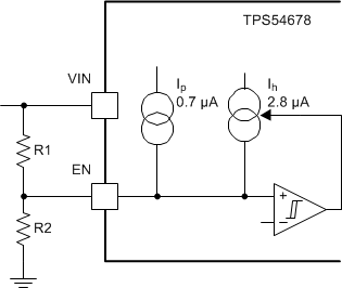
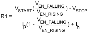
For input undervoltage lockout (UVLO), use the EN pin as shown in Figure 22 to set up the UVLO by using the two external resistors. Once the EN pin voltage exceeds 1.3 V, an additional 2.8 µA of hysteresis is added. This additional current facilitates input voltage hysteresis. Use Equation 2 to set the external hysteresis for the input voltage. Use Equation 3 to set the input startup voltage. TI recommends that the minimum input shutdown voltage be set at 2.45 V or higher to ensure proper operation before shutdown.
 Figure 22. Set Up Input Undervoltage Lockout.

where
- R1 and R2 are in Ω
- Ih = 2.8 µA
- Ip = 0.7 µA
- VEN_RISING = 1.3 V
- VEN_FALLING = 1.18 V