JAJSBO6B June 2012 – May 2019 TPS54678
PRODUCTION DATA.
- 1 特長
- 2 アプリケーション
- 3 概要
- 4 改訂履歴
- 5 概要(続き)
- 6 Pin Configuration and Functions
- 7 Specifications
-
8 Detailed Description
- 8.1 Overview
- 8.2 Functional Block Diagram
- 8.3
Feature Description
- 8.3.1 Fixed Frequency PWM Control
- 8.3.2 Slope Compensation and Output Current
- 8.3.3 Bootstrap Voltage (Boot) and Low Dropout Operation
- 8.3.4 Error Amplifier
- 8.3.5 Voltage Reference
- 8.3.6 Adjusting the Output Voltage
- 8.3.7 Enable and Adjusting Undervoltage Lockout
- 8.3.8 Soft-Start Pin
- 8.3.9 Sequencing
- 8.3.10 Constant Switching Frequency and Timing Resistor (RT/CLK Pin)
- 8.3.11 Overcurrent Protection
- 8.3.12 Safe Start-Up into Prebiased Outputs
- 8.3.13 Synchronize Using the RT/CLK Pin
- 8.3.14 Power Good (PWRGD Pin)
- 8.3.15 Overvoltage Transient Protection
- 8.3.16 Thermal Shutdown
- 8.4 Device Functional Modes
-
9 Application and Implementation
- 9.1 Application Information
- 9.2
Typical Application
- 9.2.1 Design Requirements
- 9.2.2
Detailed Design Procedure
- 9.2.2.1 Custom Design With WEBENCH® Tools
- 9.2.2.2 Step One: Select the Switching Frequency
- 9.2.2.3 Step Two: Select the Output Inductor
- 9.2.2.4 Step Three: Choose the Output Capacitor
- 9.2.2.5 Step Four: Select the Input Capacitor
- 9.2.2.6 Step Five: Choose the Soft-Start Capacitor
- 9.2.2.7 Step Six: Select the Bootstrap Capacitor
- 9.2.2.8 Step Eight: Select Output Voltage and Feedback Resistors
- 9.2.2.9 Step Nine: Select Loop Compensation Components
- 9.2.3 Application Curves
- 10Power Supply Recommendations
- 11Layout
- 12デバイスおよびドキュメントのサポート
- 13メカニカル、パッケージ、および注文情報
パッケージ・オプション
メカニカル・データ(パッケージ|ピン)
- RTE|16
サーマルパッド・メカニカル・データ
- RTE|16
発注情報
8.4.3 Small Signal Model for Frequency Compensation
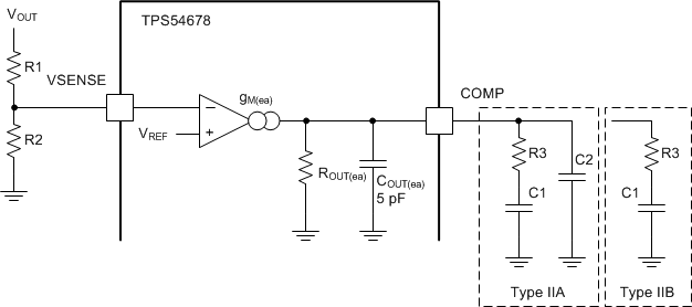
The TPS54678 uses a transconductance amplifier for the error amplifier and readily supports two of the commonly used frequency compensation circuits. The compensation circuits are shown in Figure 29. The Type 2 circuits are normally implemented in high-bandwidth power supply designs using low ESR output capacitors. In Type 2A, one additional high-frequency pole is added to attenuate high-frequency noise.
 Figure 29. Types of Frequency Compensation
 The design guidelines for TPS54678 loop compensation are as follows:
- Set up crossover frequency fc.
- R3 can be determined by Equation 10:
- gmea is the GM amplifier gain,
- gmPS is the power stage gain (20 A/V).
- Place a compensation zero at the dominant pole
 C1 can be determined by Equation 11:
 - C2 is optional. It can be used to cancel the zero from ESR of the Co in Equation 12:
Equation 10. 

where
Equation 11. 

Equation 12. 
