JAJSMU6C June 2012 – September 2021 TPS54719
PRODUCTION DATA
- 1 特長
- 2 アプリケーション
- 3 概要
- 4 Revision History
- 5 Pin Configuration and Functions
- 6 Specifications
-
7 Detailed Description
- 7.1 Overview
- 7.2 Functional Block Diagram
- 7.3
Feature Description
- 7.3.1 Fixed Frequency PWM Control
- 7.3.2 Slope Compensation And Output Current
- 7.3.3 Bootstrap Voltage (Boot) And Low Dropout Operation
- 7.3.4 Error Amplifier
- 7.3.5 Voltage Reference
- 7.3.6 Adjusting The Output Voltage
- 7.3.7 Enable and Adjusting Undervoltage Lockout
- 7.3.8 Slow Start/Tracking Pin
- 7.3.9 Sequencing
- 7.4
Device Functional Modes
- 7.4.1 Constant Switching Frequency And Timing Resistor (RT Pin)
- 7.4.2 Overcurrent Protection
- 7.4.3 Frequency Shift
- 7.4.4 Reverse Overcurrent Protection
- 7.4.5 Power Good (PWRGD Pin)
- 7.4.6 Overvoltage Transient Protection
- 7.4.7 Thermal Shutdown
- 7.4.8 Small Signal Model For Loop Response
- 7.4.9 Simple Small Signal Model For Peak Current Mode Control
- 7.4.10 Small Signal Model For Frequency Compensation
-
8 Application and Implementation
- 8.1 Application Information
- 8.2
Typical Application
- 8.2.1 High Frequency, 1.8-V Output Power Supply Design With Adjusted UVLO
- 8.2.2 Design Requirements
- 8.2.3
Detailed Design Procedure
- 8.2.3.1 Selecting The Switching Frequency
- 8.2.3.2 Output Inductor Selection
- 8.2.3.3 Output Capacitor
- 8.2.3.4 Input Capacitor
- 8.2.3.5 Slow-Start Capacitor
- 8.2.3.6 Bootstrap Capacitor Selection
- 8.2.3.7 Undervoltage Lockout Set Point
- 8.2.3.8 Output Voltage And Feedback Resistors Selection
- 8.2.3.9 Compensation
- 8.2.4 Application Curves
- 9 Power Supply Recommendations
- 10Layout
- 11Device and Documentation Support
- 12Mechanical, Packaging, and Orderable Information
パッケージ・オプション
メカニカル・データ(パッケージ|ピン)
- RTE|16
サーマルパッド・メカニカル・データ
- RTE|16
発注情報
7.3.7 Enable and Adjusting Undervoltage Lockout
The TPS54719 is disabled when the VIN pin voltage falls below 2.2 V. If an application requires a higher undervoltage lockout (UVLO), use the EN pin as shown in Figure 7-2 to adjust the input voltage UVLO by using two external resistors. It is recommended to use the enable resistors to set the UVLO falling threshold (VSTOP) above 2.7 V. The rising threshold (VSTART) should be set to provide enough hysteresis to allow for any input supply variations. The EN pin has an internal pullup current source that provides the default condition of the TPS54719 operating when the EN pin floats. Once the EN pin voltage exceeds 1.25 V, an additional 2.9 μA of hysteresis is added. When the EN pin is pulled below 1.18 V, the 2.9 μA is removed. This additional current facilitates input voltage hysteresis.
 Figure 7-2 Adjustable Undervoltage
Lockout
Figure 7-2 Adjustable Undervoltage
Lockout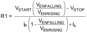
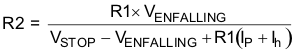
where:
- Ih = 2.9 µA
- IP = 0.7 µA
- VENRISING = 1.25 V
- VENFALLING = 1.18 V