SLVSA31A November 2009 – December 2014 TPS61029-Q1
PRODUCTION DATA.
- 1 Features
- 2 Applications
- 3 Description
- 4 Simplified Schematic
- 5 Revision History
- 6 Device Comparison Table
- 7 Pin Configuration and Functions
- 8 Specifications
- 9 Typical Characteristics
- 10Parameter Measurement Information
- 11Detailed Description
- 12Application and Implementation
- 13Power Supply Recommendations
- 14Layout
- 15Device and Documentation Support
- 16Mechanical, Packaging, and Orderable Information
パッケージ・オプション
デバイスごとのパッケージ図は、PDF版データシートをご参照ください。
メカニカル・データ(パッケージ|ピン)
- DPN|10
- DRC|10
サーマルパッド・メカニカル・データ
- DRC|10
発注情報
12 Application and Implementation
NOTE
Information in the following applications sections is not part of the TI component specification, and TI does not warrant its accuracy or completeness. TI’s customers are responsible for determining suitability of components for their purposes. Customers should validate and test their design implementation to confirm system functionality.
12.1 Application Information
The devices are designed to operate from an input voltage supply range between 0.9 V (Vin rising UVLO is 1.2V) and 6.5 V with a maximum switching current limit up to 1.8A. The devices operate in PWM mode for medium to heavy load conditions and in power save mode at light load currents. In PWM mode the TPS6102x converter operates with the nominal switching frequency of 600kHz typically. As the load current decreases, the converter enters power save mode, reducing the switching frequency and minimizing the IC quiescent current to achieve high efficiency over the entire load current range. The Power Save mode can be disabled when connecting PS pin to logic high, forcing the converter to operate at a fixed switching frequency.
12.1.1 Application Examples
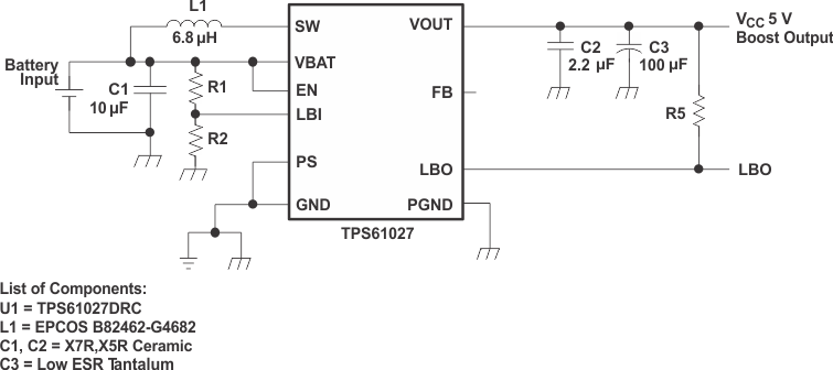 Figure 11. Power Supply Solution for Maximum Output Power Operating From a Single Alkaline Cell
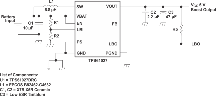 Figure 12. Power Supply Solution for Maximum Output Power Operating From a Dual/Triple Alkaline Cell or Single Li-Ion Cell
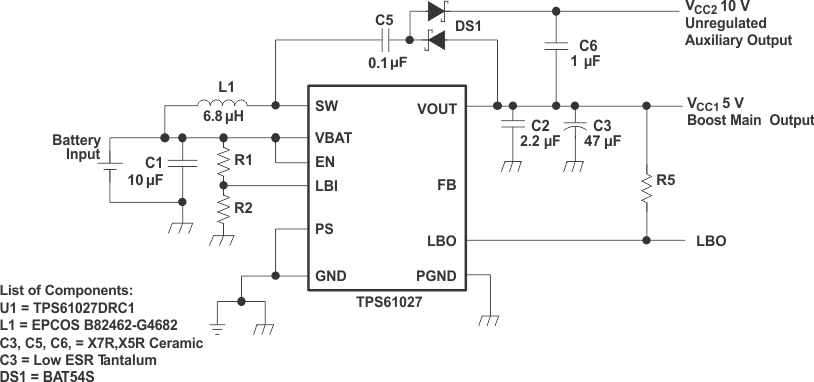 Figure 13. Power Supply Solution With Auxiliary Positive Output Voltage
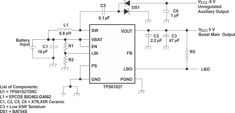 Figure 14. Power Supply Solution With Auxiliary Negative Output Voltage
12.2 Typical Application
TPS6102x with 1.2V-6.5 VIN, 800 mA Output Current
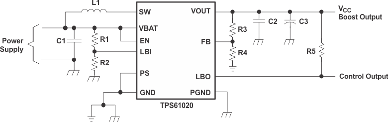 Figure 15. Typical Application Circuit for Adjustable Output Voltage Option
12.2.1 Design Requirements
The TPS6102x dc/dc converters are intended for systems powered by a single up to triple cell Alkaline, NiCd, NiMH battery with a typical terminal voltage between 0.9 V and 6.5 V. They can also be used in systems powered by one-cell Li-Ion or Li-Polymer with a typical voltage between 2.5 V and 4.2 V. Additionally, any other voltage source with a typical output voltage between 0.9 V and 6.5 V can power systems where the TPS6102x is used.
12.2.1.1 Inductor Selection
A boost converter normally requires two main passive components for storing energy during the conversion. A boost inductor and a storage capacitor at the output are required. To select the boost inductor, it is recommended to keep the possible peak inductor current below the current limit threshold of the power switch in the chosen configuration. For example, the current limit threshold of the TPS6102xs switch is 1800 mA at an output voltage of 5 V. The highest peak current through the inductor and the switch depends on the output load, the input (VBAT), and the output voltage (VOUT). Estimation of the maximum average inductor current can be done using Equation 4:
For example, for an output current of 200 mA at 3.3 V, at least 920 mA of average current flows through the inductor at a minimum input voltage of 0.9 V.
The second parameter for choosing the inductor is the desired current ripple in the inductor. Normally, it is advisable to work with a ripple of less than 20% of the average inductor current. A smaller ripple reduces the magnetic hysteresis losses in the inductor, as well as output voltage ripple and EMI. But in the same way, regulation time at load changes rises. In addition, a larger inductor increases the total system costs. With those parameters, it is possible to calculate the value for the inductor by using Equation 5:
Parameter f is the switching frequency and ΔIL is the ripple current in the inductor, i.e., 20% × IL. In this example, the desired inductor has the value of 5.5 µH. With this calculated value and the calculated currents, it is possible to choose a suitable inductor. In typical applications a 6.8 µH inductance is recommended. The device has been optimized to operate with inductance values between 2.2 µH and 22 µH. Nevertheless operation with higher inductance values may be possible in some applications. Detailed stability analysis is then recommended. Care has to be taken that load transients and losses in the circuit can lead to higher currents as estimated in Equation 5. Also, the losses in the inductor caused by magnetic hysteresis losses and copper losses are a major parameter for total circuit efficiency.
The following inductor series from different suppliers have been used with the TPS6102x converters:
Table 1. List of Inductors(1)
| SUPPLIER | INDUCTOR SERIES |
|---|---|
| Sumida | CDRH4D28 |
| CDRH5D28 | |
| Wurth Elektronik | 7447789 |
| 744042 | |
| EPCOS | B82462-G4 |
| Cooper Electronics Technologies | SD25 |
| SD20 |
12.2.1.2 Input Capacitor
At least a 10-µF input capacitor is recommended to improve transient behavior of the regulator and EMI behavior of the total power supply circuit. A ceramic capacitor or a tantalum capacitor with a 100-nF ceramic capacitor in parallel, placed close to the IC, is recommended.
12.2.1.3 Output Capacitor
The major parameter necessary to define the output capacitor is the maximum allowed output voltage ripple of the converter. This ripple is determined by two parameters of the capacitor, the capacitance and the ESR. It is possible to calculate the minimum capacitance needed for the defined ripple, supposing that the ESR is zero, by using Equation 6:
Parameter f is the switching frequency and ΔV is the maximum allowed ripple.
With a chosen ripple voltage of 10 mV, a minimum capacitance of 24 µF is needed. The total ripple is larger due to the ESR of the output capacitor. This additional component of the ripple can be calculated using Equation 7:
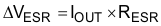
An additional ripple of 16 mV is the result of using a tantalum capacitor with a low ESR of 80 mΩ. The total ripple is the sum of the ripple caused by the capacitance and the ripple caused by the ESR of the capacitor. In this example, the total ripple is 26 mV. Additional ripple is caused by load transients. This means that the output capacitor has to completely supply the load during the charging phase of the inductor. A reasonable value of the output capacitance depends on the speed of the load transients and the load current during the load change. With the calculated minimum value of 24 µF and load transient considerations the recommended output capacitance value is in a 47 to 100 µF range. For economical reasons, this is usually a tantalum capacitor. Therefore, the control loop has been optimized for using output capacitors with an ESR of above 30 mΩ. The minimum value for the output capacitor is 10 µF.
12.2.2 Detailed Design Procedure
12.2.2.1 Small Signal Stability
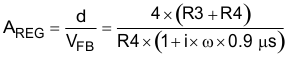
When using output capacitors with lower ESR, like ceramics, the adjustable voltage version is recommended. The missing ESR can be compensated in the feedback divider. Typically a capacitor in the range of 4.7 pF in parallel to R3 helps to obtain small signal stability with lowest ESR output capacitors. For more detailed analysis, the small signal transfer function of the error amplifier and the regulator, which is given in Equation 8, can be used:
12.2.2.2 Thermal Information
Implementation of integrated circuits in low-profile and fine-pitch surface-mount packages typically requires special attention to power dissipation. Many system-dependent issues such as thermal coupling, airflow, added heat sinks and convection surfaces, and the presence of other heat-generating components affect the power-dissipation limits of a given component.
Three basic approaches for enhancing thermal performance are listed below.
- Improving the power dissipation capability of the PCB design
- Improving the thermal coupling of the component to the PCB
- Introducing airflow in the system
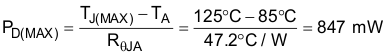
The maximum recommended junction temperature (TJ) of the TPS6102x devices is 125°C. The thermal resistance of the 10-pin QFN 3 × 3 package (DRC) is RΘJA = 47.2°C/W, if the PowerPAD is soldered. Specified regulator operation is assured to a maximum ambient temperature TA of 85°C. Therefore, the maximum power dissipation is about 847 mW. More power can be dissipated if the maximum ambient temperature of the application is lower.
12.2.3 Application Curves
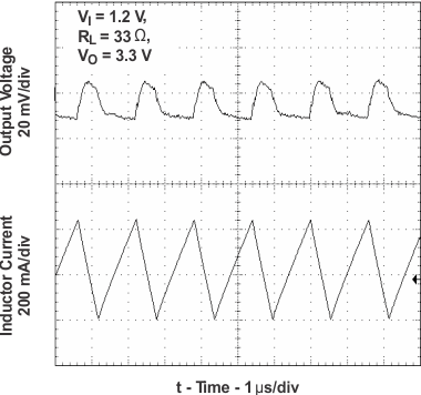 Figure 16. TPS61025 Output Voltage In Continuous Mode
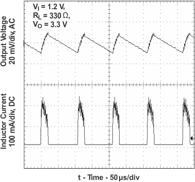 Figure 18. TPS61025 Output Voltage In Power Save Mode
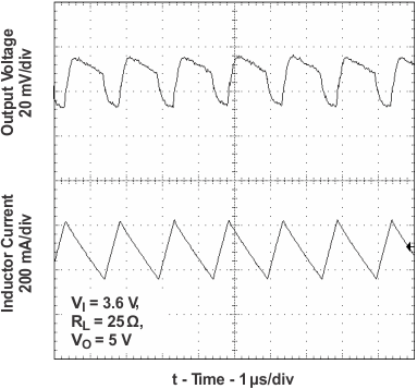 Figure 17. TPS61027 Output Voltage In Continuous Mode
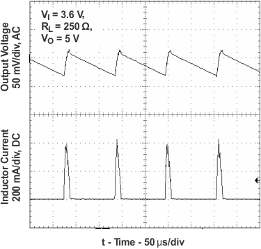 Figure 19. TPS61027 Output Voltage In Power Save Mode
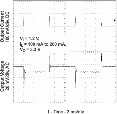 Figure 20. TPS61025 Load Transient Response
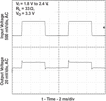 Figure 22. TPS61025 Line Transient Response
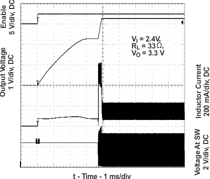 Figure 24. TPS61025 Start-Up After Enable
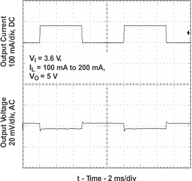 Figure 21. TPS61027 Load Transient Response
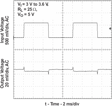 Figure 23. TPS61027 Line Transient Response
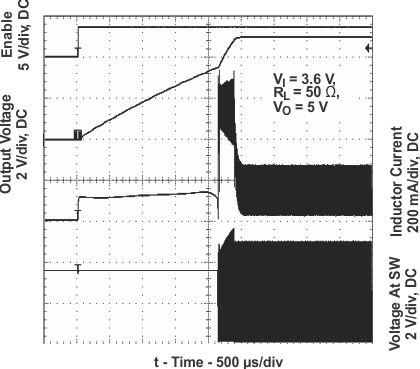 Figure 25. TPS61027 Start-Up After Enable