SLVSA31A November 2009 – December 2014 TPS61029-Q1
PRODUCTION DATA.
- 1 Features
- 2 Applications
- 3 Description
- 4 Simplified Schematic
- 5 Revision History
- 6 Device Comparison Table
- 7 Pin Configuration and Functions
- 8 Specifications
- 9 Typical Characteristics
- 10Parameter Measurement Information
- 11Detailed Description
- 12Application and Implementation
- 13Power Supply Recommendations
- 14Layout
- 15Device and Documentation Support
- 16Mechanical, Packaging, and Orderable Information
パッケージ・オプション
デバイスごとのパッケージ図は、PDF版データシートをご参照ください。
メカニカル・データ(パッケージ|ピン)
- DPN|10
- DRC|10
サーマルパッド・メカニカル・データ
- DRC|10
発注情報
9 Typical Characteristics
Table of Graphs
| FIGURE | ||
|---|---|---|
| Maximum output current | vs Input voltage | Figure 1 |
| Efficiency | vs Output current (TPS61025) | Figure 2 |
| vs Output current (TPS61027) | Figure 3 | |
| vs Input voltage (TPS61025) | Figure 4 | |
| vs Input voltage (TPS61027) | Figure 5 | |
| Output voltage | vs Output current (TPS61025) | Figure 6 |
| vs Output current (TPS61027) | Figure 7 | |
| No load supply current into VBAT | vs Input voltage | Figure 8 |
| No load supply current into VOUT | vs Input voltage | Figure 9 |
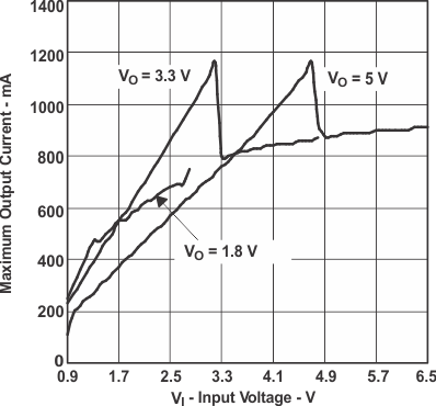 Figure 1. Maximum Output Current vs Input Voltage
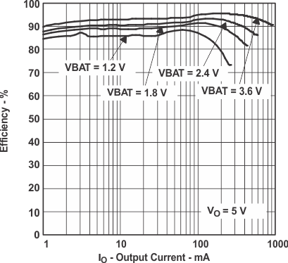 Figure 3. TPS61027 Efficiency vs Output Current
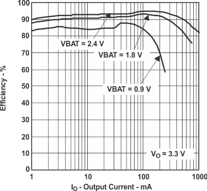 Figure 2. TPS61025 Efficiency vs Output Current
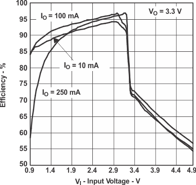 Figure 4. TPS61025 Efficiency vs Input Voltage
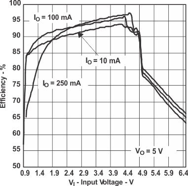 Figure 5. TPS61027 Efficiency vs Input Voltage
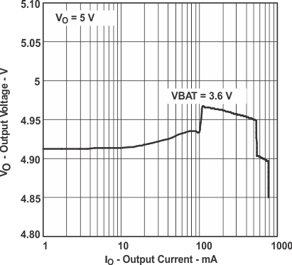 Figure 7. TPS61027 Output Voltage vs Output Current
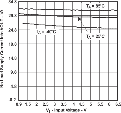 Figure 9. No Load Supply Current Into VOUT vs Input Voltage
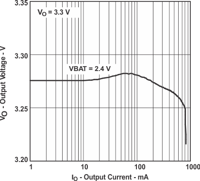 Figure 6. TPS61025 Output Voltage vs Output Current
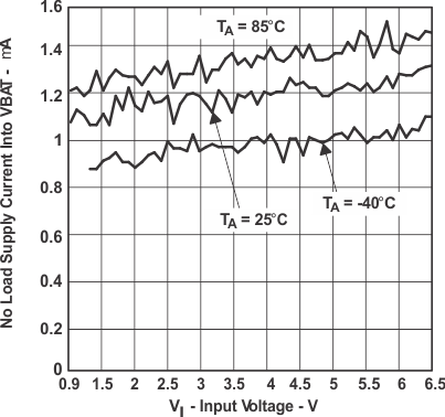 Figure 8. No Load Supply Current Into VBAT vs Input Voltage