SLVSA31A November 2009 – December 2014 TPS61029-Q1
PRODUCTION DATA.
- 1 Features
- 2 Applications
- 3 Description
- 4 Simplified Schematic
- 5 Revision History
- 6 Device Comparison Table
- 7 Pin Configuration and Functions
- 8 Specifications
- 9 Typical Characteristics
- 10Parameter Measurement Information
- 11Detailed Description
- 12Application and Implementation
- 13Power Supply Recommendations
- 14Layout
- 15Device and Documentation Support
- 16Mechanical, Packaging, and Orderable Information
パッケージ・オプション
デバイスごとのパッケージ図は、PDF版データシートをご参照ください。
メカニカル・データ(パッケージ|ピン)
- DPN|10
- DRC|10
サーマルパッド・メカニカル・データ
- DRC|10
発注情報
7 Pin Configuration and Functions
VSON (DRC) (DPN)
10-Pin Package
TOP VIEW
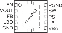
Pin Functions
| PIN | I/O | DESCRIPTION | |
|---|---|---|---|
| NAME | NO. | ||
| EN | 1 | I | Enable input (1/VBAT enabled, 0/GND disabled) |
| FB | 3 | I | Voltage feedback of adjustable versions |
| GND | 5 | Control / logic ground | |
| LBI | 7 | I | Low battery comparator input (comparator enabled with EN), may not be left floating, should be connected to GND or VBAT if comparator is not used |
| LBO | 4 | O | Low battery comparator output (open drain) |
| PS | 8 | I | Enable/disable power save mode (1/VBAT disabled, 0/GND enabled) |
| SW | 9 | I | Boost and rectifying switch input |
| PGND | 10 | Power ground | |
| VBAT | 6 | I | Supply voltage |
| VOUT | 2 | O | Boost converter output |
| PowerPAD™ | Must be soldered to achieve appropriate power dissipation. Should be connected to PGND. | ||