JAJSFK4A September   2018  – November 2018 TPS61088-Q1

PRODUCTION DATA.  

  1. 特長
  2. アプリケーション
  3. 概要
    1.     Device Images
      1.      代表的なアプリケーション回路
  4. 改訂履歴
  5. 概要(続き)
  6. Pin Configuration and Functions
    1.     Pin Functions
  7. Specifications
    1. 7.1 Absolute Maximum Ratings
    2. 7.2 ESD Ratings
    3. 7.3 Recommended Operating Conditions
    4. 7.4 Thermal Information
    5. 7.5 Electrical Characteristics
    6. 7.6 Typical Characteristics
  8. Detailed Description
    1. 8.1 Overview
    2. 8.2 Functional Block Diagram
    3. 8.3 Feature Description
      1. 8.3.1 Enable and Start-up
      2. 8.3.2 Undervoltage Lockout (UVLO)
      3. 8.3.3 Adjustable Switching Frequency
      4. 8.3.4 Adjustable Peak Current Limit
      5. 8.3.5 Overvoltage Protection
      6. 8.3.6 Thermal Shutdown
    4. 8.4 Device Functional Modes
      1. 8.4.1 Operation
        1. 8.4.1.1 PWM Mode
        2. 8.4.1.2 PFM Mode
  9. Application and Implementation
    1. 9.1 Application Information
    2. 9.2 Typical Application
      1. 9.2.1 Design Requirements
      2. 9.2.2 Detailed Design Procedure
        1. 9.2.2.1 Custom Design with WEBENCH Tools
        2. 9.2.2.2 Setting Switching Frequency
        3. 9.2.2.3 Setting Peak Current Limit
        4. 9.2.2.4 Setting Output Voltage
        5. 9.2.2.5 Inductor Selection
        6. 9.2.2.6 Input Capacitor Selection
        7. 9.2.2.7 Output Capacitor Selection
        8. 9.2.2.8 Loop Stability
      3. 9.2.3 Application Curves
  10. 10Power Supply Recommendations
  11. 11Layout
    1. 11.1 Layout Guidelines
    2. 11.2 Layout Example
    3. 11.3 Thermal Considerations
  12. 12デバイスおよびドキュメントのサポート
    1. 12.1 デバイス・サポート
      1. 12.1.1 デベロッパー・ネットワークの製品に関する免責事項
      2. 12.1.2 開発サポート
        1. 12.1.2.1 WEBENCHツールによるカスタム設計の作成
    2. 12.2 ドキュメントの更新通知を受け取る方法
    3. 12.3 コミュニティ・リソース
    4. 12.4 商標
    5. 12.5 静電気放電に関する注意事項
    6. 12.6 Glossary
  13. 13メカニカル、パッケージ、および注文情報

パッケージ・オプション

メカニカル・データ(パッケージ|ピン)
サーマルパッド・メカニカル・データ
発注情報

Setting Peak Current Limit

The peak input current is set by selecting the correct external resistor value correlating to the required current limit. Because the TPS61088-Q1 is configured to work in the PFM mode in light load condition, use Equation 6 to calculate the correct resistor value:
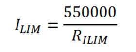
Equation 6. TPS61088-Q1 TPS61088-Q1_ILIM_EQU_update.gif

where

  • RILIM is the resistance connected between the ILIM pin and ground.
  • ILIM is the switching peak current limit.

For a typical current limit of 11.0 A, the resistor value is 49.9 kΩ. Considering the device variation and the tolerance over temperature, the minimum current limit at the worst case can be 1.3 A lower than the value calculated by Equation 6. The minimum current limit must be higher than the required peak switch current at the lowest input voltage and the highest output power to make sure the TPS61088-Q1 does not hit the current limit and still can regulate the output voltage in these conditions.