SLVSAG3A September 2010 – December 2014 TPS61252
PRODUCTION DATA.
- 1 Features
- 2 Applications
- 3 Description
- 4 Typical Application Schematic
- 5 Revision History
- 6 Device Options
- 7 Pin Configuration and Functions
- 8 Specifications
- 9 Parameter Measurement Information
- 10Detailed Description
- 11Application and Implementation
- 12Power Supply Recommendations
- 13Layout
- 14Device and Documentation Support
- 15Mechanical, Packaging, and Orderable Information
11 Application and Implementation
NOTE
Information in the following applications sections is not part of the TI component specification, and TI does not warrant its accuracy or completeness. TI’s customers are responsible for determining suitability of components for their purposes. Customers should validate and test their design implementation to confirm system functionality.
11.1 Application Information
The TPS61252 device provides a power supply solution for products powered by either a three-cell alkaline, NiCd or NiMH battery, or an one-cell Li-Ion or Li-polymer battery. The wide input voltage range is ideal to power portable applications like mobile phones or for computer peripherals. TPS61252 allows the use of small inductors and input capacitors to achieve a small solution size. The possibility to reduce the current limit by a external resistor offers the potential use of physically even smaller inductors with lower rated current to further reduce total solution sizes of the power supply.
11.2 Typical Application
Typical application for 5-V output voltage with input current limit.
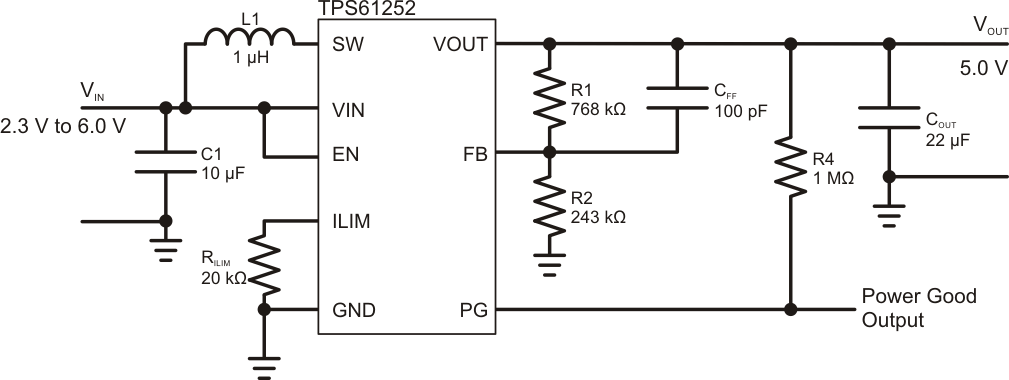 Figure 9. Typical Application Circuit for 5-V Output Voltage
11.2.1 Design Requirements
In this example, use the TPS61252 to design a 5-V output power supply supporting customer required input current limit, input voltage range and output driving capability. Below specific example will be used to define and work with the different equations.
Table 2. Design Parameters
| PARAMETER | VALUE | UNIT | |
|---|---|---|---|
| VIN | Input Voltage | 3.6 | V |
| VIN(min) | Minimum Input Voltage | 2.6 | V |
| VOUT | Output Voltage | 5.0 | V |
| ILIM | Input Current Limit set by RILIM | 1000 | mA |
| VFB | Feedback Voltage | 1.2 | V |
| f | Switching Frequency | 3.25 | MHz |
| η | Estimated Efficiency | 90 | % |
| L1 | Inductor Value of Choice | 1.0 | µH |
11.2.2 Detailed Design Procedure
Table 3. List of Components
11.2.2.1 Output Voltage Setting
The output voltage is calculated by Equation 5:
To minimize the current through the feedback divider network, R2 should be between 180 kΩ and 360 kΩ. The sum of R1 and R2 should not exceed ~1 MΩ, to keep the network robust against noise. For the example, R1 is 768 kΩ and R2 is 243 kΩ.
An external feed forward capacitor C1 is required for optimum load transient response. The value of C1 should be 100 pF. The connection from the FB pin to the resistor divider should be kept short and away from noise sources, such as the inductor or the SW line.
11.2.2.2 Input Current Limit
The input current limit is set by selecting the correct external resistor value. Equation 6 is a guideline for selecting the correct resistor value:
For a current limit of 1 A, the resistor value is 10 kΩ.
To allow maximum current limit the ILIM pin can be directly connected to VIN.
11.2.2.3 Maximum Output Current
The maximum output current is set by RILIM and the input to output voltage ratio and can be calculated by Equation 7:
Following the example IOUT(max) is 648 mA at 3.6 V input voltage and decreases, with lower input voltage values.
11.2.2.4 Inductor Selection
As for all switching power supplies two main passive components are required for storing the energy during operation: an inductor and an output capacitor. The inductor must be connected between the VIN pin and SW pin to make sure that the TPS61252 device operates. To select the right inductor current rating, the programmed input current limit as well as the current ripple through the inductor should be calculated. An estimation of the maximum peak inductor current can be done using Equation 8.
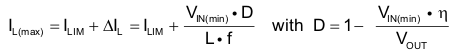
Regarding the above example the current ripple (ΔIL) is 426 mA and therefore an inductor with a rated current of about 1.5 A should be used.
The TPS61252 is designed to work with inductor values between 1.0 µH and 2.2 µH. For typical applications, a 1.5 µH inductor is recommended. In space constrained applications, it might be possible to consider smaller inductor values depending on the targeted inductor ripple current. Therefore the inductor value can be reduced down to 1.0 µH without degrading the stability.
In regular boost converter designs the current through the inductor is defined by the fixed switch current limit of the converter's switches and therefore bigger inductors have to be chosen. The TPS61252 allows the design engineer to reduce the current limit to the needs of the application regardless the maximum switch current limit of the converter. Programming a lower current value allows the use of smaller inductors without the danger of saturation.
11.2.2.5 Output Capacitor
For the output capacitor, it is recommended to use small X5R or X7R ceramic capacitors placed as close as possible to the VOUT and GND pins of the IC. If, for any reason, the application requires the use of large capacitors which cannot be placed close to the IC, a smaller ceramic capacitor in parallel to the large one is required. This small capacitor should be placed as close as possible to the converter's VOUT and GND pins.
To maintain control loop stability of the boost converter, a minimum effective output capacitance of at least 8 µF is recommended. That means due to DC Bias effect (see NOTE) a 22 µF capacitor with 0805 case size and a voltage rating of 10 V is necessary. In height restricted application two 10 µF capacitors with 0603 case size and 6.3 V voltage rating can also be used.
In addition to the minimum COUT the application might need more capacitance. To get an estimate of the minimum output capacitance necessary for the application, Equation 9 is used:
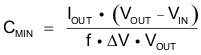
Where ΔV is the maximum allowed output ripple.
With a chosen ripple voltage of 10 mV, a minimum effective capacitance of 9.6 μF is needed regarding the example. The total ripple is larger due to the ESR of the output capacitor. This additional component of the ripple can be calculated using Equation 10:

11.2.2.6 Input Capacitor
Multilayer X5R or X7R ceramic capacitors are an excellent choice for input decoupling of the step-up converter as they have extremely low ESR and are available in small form factors. The input capacitors should be located as close as possible to the device. While a 10μF input capacitor is sufficient for most applications, larger values may be used to reduce input current ripple. Also, low ESR tantalum capacitors may be used.
NOTE
DC Bias effect: High capacitance ceramic capacitors have a DC Bias effect, which has a strong influence on the final effective capacitance. Therefore the right capacitor value has to be chosen very carefully. Package size and voltage rating in combination with dielectric material are responsible for differences between the rated capacitor value and the effective capacitance. A 10 V rated 0805 capacitor with 10 µF can have a effective capacitance of less than 5 µF at an output voltage of 5 V.
11.2.2.7 Checking Loop Stability
The first step of circuit and stability evaluation is to look from a steady-state perspective at the following signals:
- Switch node, SW
- Inductor current, IL
- Output ripple voltage, VOUT(AC)
These are the basic signals that need to be measured when evaluating a switching converter. When the switching waveform shows large duty cycle jitter or the output voltage or inductor current shows oscillations, the regulation loop may be unstable. This is often a result of board layout and/or L-C combination.
As the next step in the evaluation of the regulation loop, the load transient response is tested. During the time between when the load transient takes place and the turn on of the high side switch, the output capacitor must supply all of the current required by the load. VOUT immediately shifts by an amount equal to ΔI(LOAD) x ESR, where ESR is the effective series resistance of COUT. ΔI(LOAD) begins to charge or discharge COUT, generating a feedback error signal used by the regulator to return VOUT to its steady-state value. The results are most easily interpreted when the device operates in PWM mode.
During this recovery time, VOUT can be monitored for settling time, overshoot or ringing that helps judge the converter’s stability. Without any ringing, the loop has usually more than 60° of phase margin. Because the damping factor of the circuitry is directly related to several resistive parameters (for example, MOSFET rDS(on)) that are temperature dependant, the loop stability analysis has to be done over the input voltage range, load current range, and temperature range.
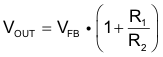
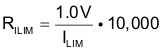
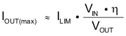
11.2.3 Application Curves
| FIGURE | |
|---|---|
| Load transient response (VIN = 3.6 V, VOUT = 5.0V, ILIM = 500mA, Load change from 20 mA to 300 mA) | Figure 10 |
| Load transient response (VIN = 3.6 V, VOUT = 5.0V, VIN > VOUT, ILIM = 1000mA, Load change from 50 mA to 550 mA) | Figure 11 |
| Startup after enable (VOUT = 5.0 V, VIN = 3.6 V, ILIM = 500mA) | Figure 12 |
| Startup after enable (VOUT = 5.0 V, VIN = 3.6 V, ILIM = 1000mA) | Figure 13 |
| Startup after enable in 500 mA load (VOUT = 5.0 V, VIN = 3.6 V, ILIM = 1000mA) | Figure 14 |
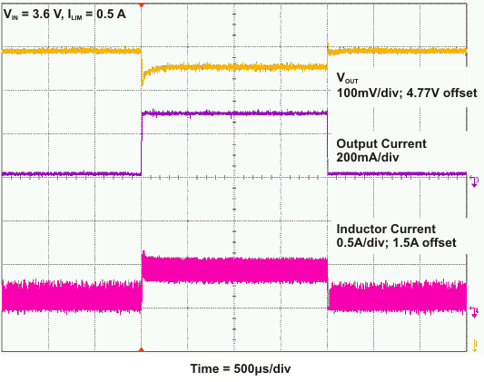 Figure 10. Load Transient Response ILIM = 500 mA (20 to 300 mA)
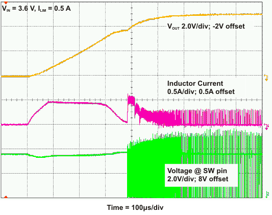 Figure 12. Startup After Enable ILIM = 500mA, No Load
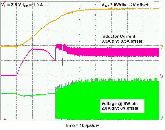 Figure 14. Startup After Enable ILIM = 1000mA, 500 mA Load
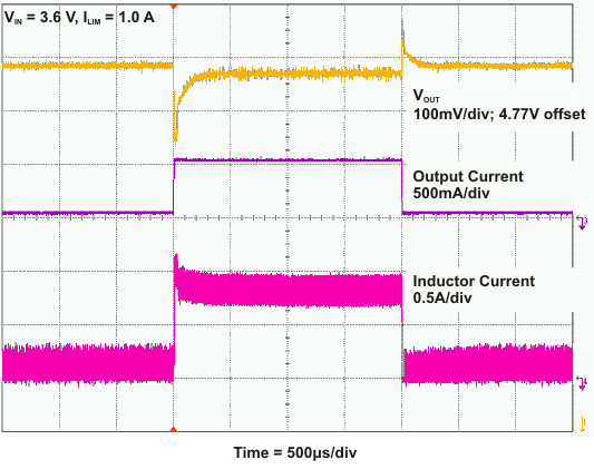 Figure 11. Load Transient Response ILIM = 1000 mA (50 to 550 mA)
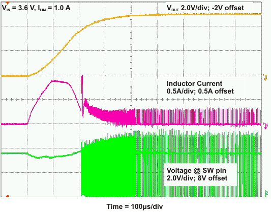 Figure 13. Startup After Enable ILIM = 1000mA, NO Load