SLVSAG3A September 2010 – December 2014 TPS61252
PRODUCTION DATA.
- 1 Features
- 2 Applications
- 3 Description
- 4 Typical Application Schematic
- 5 Revision History
- 6 Device Options
- 7 Pin Configuration and Functions
- 8 Specifications
- 9 Parameter Measurement Information
- 10Detailed Description
- 11Application and Implementation
- 12Power Supply Recommendations
- 13Layout
- 14Device and Documentation Support
- 15Mechanical, Packaging, and Orderable Information
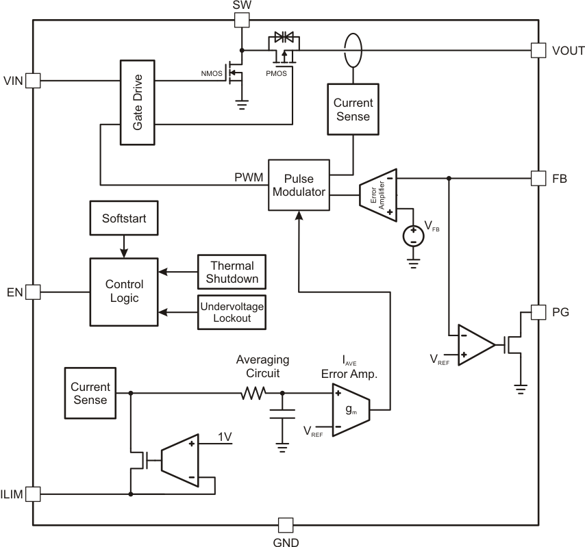
10 Detailed Description
10.1 Overview
The TPS61252 device provides a power supply solution for products powered by either a three-cell alkaline, NiCd or NiMH battery, or an one-cell Li-Ion or Li-polymer battery. It has a resistor programmable (RILIM) input current limit. During light loads the device will automatically enter skip mode (PFM). During shutdown, the load is completely disconnected from the battery.
10.2 Functional Block Diagram
10.3 Feature Description
10.3.1 Operation
The TPS61252 boost converter operates as a quasi-constant frequency adaptive on-time controller. In a typical application, the frequency is 3.25 MHz and is defined by the input to output voltage ratio and does not vary from moderate to heavy load currents. At light load currents, the converter automatically enters Power Save Mode and operates in PFM (Pulse Frequency Modulation) mode. During pulse-width-modulation (PWM) operation, the converter uses a unique fast response quasi-constant on-time valley current mode controller scheme which offers very good line and load regulation allowing the use of small ceramic input and output capacitors.
Based on the VIN/VOUT ratio, a simple circuit predicts the required on-time. At the beginning of the switching cycle, the low-side N-MOS switch is turned-on and the inductor current ramps up to a peak current that is defined by the on-time and the inductance. In the second phase, once the on-timer has expired, the rectifier is turned-on and the inductor current decays to a preset valley current threshold. Finally, the switching cycle repeats by setting the on-timer again and activating the low-side N-MOS switch.
The TPS61252 controls the input current through an intelligent adjustment of a valley current limit that corrects the value in a way that it almost turns out as an average input current limit. The current can be adjusted with an accuracy of ±20%.
This architecture with adaptive slope compensation provides excellent transient load response and requires minimal output filtering. Internal softstart and loop compensation simplifies the design process, while minimizing the number of external components.
10.3.2 Current Limit Operation
The current limit circuit employs a valley current sensing scheme. Current limit detection occurs during the off time, through sensing of the voltage drop across the synchronous rectifier.
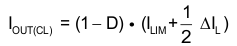
The output voltage is reduced when the power stage of the device operates in a constant current mode. The maximum continuous output current (IOUT(CL)), before entering current limit (CL) operation, can be defined by Equation 1.
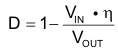
The duty cycle (D) can be estimated by Equation 2:
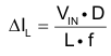
and the peak-to-peak current ripple (ΔIL) is calculated by Equation 3:
The output current, IOUT(LIM), is the average of the rectifier current waveform. When the load current is increased such that the lower peak is above the current limit threshold, the off-time is increased to allow the current to decrease to this threshold before the next on-time begins. When the current limit is reached, the output voltage decreases if the load is further increased.
10.3.3 Softstart
The TPS61252 has an internal softstart circuit that controls the ramp-up of the current during start-up and prevents the converter from inrush current that exceeds the set current limit. The current is ramped to the set current limit in typical 100 µs . After reaching the current limit threshold, it stays there until VIN = VOUT then the converter starts switching and boosting up the voltage to its nominal output voltage. During the complete start-up, the input current does not exceed the current limit that is set by resistor RILIM.
10.3.4 Enable
The device is enabled by setting the EN pin to a voltage above 1 V. At first, the internal reference is activated and the internal analog circuits are settled. After typically 50 µs, the output voltage ramps up, controlled by the softstart circuitry. The output voltage reaches its nominal value as fast as the current limit settings and the load condition allows it.
The EN input can be used to control power sequencing in a system with several DC-DC converters. The EN pin can be connected to the output of another converter, to drive the EN pin high and get a sequencing of supply rails. With EN = GND, the device enters shutdown mode. Do not leave the enable pin floating.
10.3.5 Under-Voltage Lockout (UVLO)
The under voltage lockout circuit prevents the device from malfunctioning at low input voltages and the battery from excessive discharge. It disables the output stage of the converter once the falling VIN trips the under-voltage lockout threshold VUVLO which is typically 2.0V. The device starts operation again once the rising VIN trips the VUVLO threshold plus its hysteresis of typically 100 mV.
10.3.6 Power Good
The device has a built in power good function to indicate whether the output voltage operates within appropriate levels. The PG pin is an open drain output, requiring a pull-up resistor. If the PG pin is not used, it may be left floating or connected to GND. The power good output (PG) is set floating after the FB pin voltage reaches 95% of its nominal value and stays there until the feedback voltage falls below 90 % of the nominal value. The power good is operable as long as the converter is enabled and VIN is present. If the converter is disabled by pulling the EN pin low the PG open drain output is high impedance. That means it follows the voltage it is connected to via the pull-up resistor. If the converter is controlled by an external enable signal and the power good should indicate that the output is turned off the application circuit below should be used. In the following circuit, the EN pin voltage provides the high level for the PG pin pull-up resistor R4.
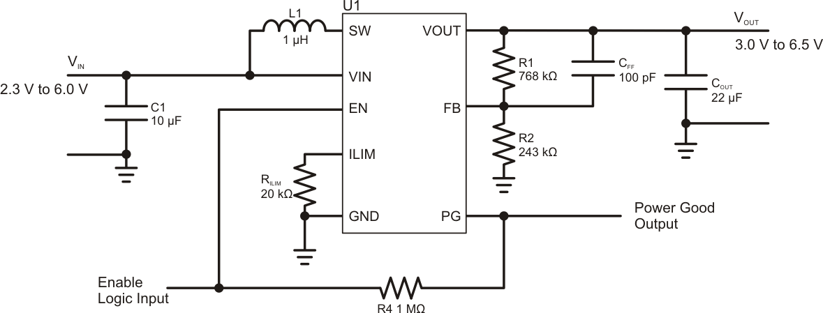 Figure 7. Power Good Schematic
10.3.7 Input Over Voltage Protection
This converter has input over voltage protection that protects the device from damage due to a voltage higher than the absolute maximum rating on the VIN pin. If 6.5 V (typical) at the input is exceeded, the converter completely shuts down to protect its inner circuitry. If the input voltage drops below 6.4 V (typical), it turns on the device again and enters normal start up.
10.3.8 Load Disconnect and Reverse Current Protection
Regular boost converters do not disconnect the load from the input supply and therefore a connected battery is discharged during shutdown. The advantage of the TPS61252 is that this converter disconnects the output from the input of the power supply when it is disabled. In case of a connected battery, it prevents it from being discharged during shutdown of the converter. Furthermore, the output is not allowed to pass current to the input (battery).
10.3.9 Thermal Regulation
The TPS61252 contains a thermal regulation loop that monitors the die temperature. If the die temperature rises to values above 110 °C, the device automatically reduces the current limit to prevent the die temperature from further increasing. Once the die temperature drops about 10 °C below the threshold, the device automatically increases the current to the set value. This function also reduces the current during a short-circuit-condition.
10.3.10 Thermal Shutdown
As soon as the junction temperature, TJ, exceeds 140°C (typical), the device enters thermal shutdown. In this mode, the High Side and Low Side MOSFETs are turned-off. When the junction temperature falls about 20 °C below the thermal shutdown, the device resumes operation.
10.4 Device Functional Modes
10.4.1 Power Save Mode
The TPS61252 integrates a power save mode to improve efficiency at light load. In power save mode the converter only operates when the output voltage trips below a set threshold voltage. It ramps up the output voltage with several pulses and goes into power save mode again once the output voltage exceeds the set threshold voltage. During the power save operation when the output voltage is above the set threshold, the converter turns off some of the inner circuits to save energy.
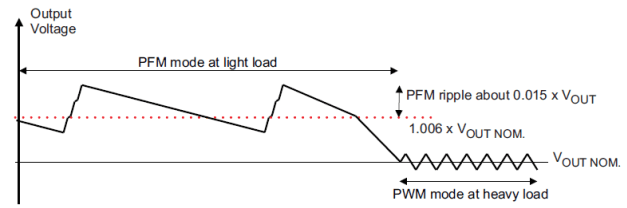 Figure 8. Power Save Mode
The PFM mode is left and PWM mode entered, in case the output current can no longer be supported in PFM mode.
10.4.2 100% Duty-Cycle Mode
If VIN > VOUT, the TPS61252 offers the lowest possible input-to-output voltage difference while still maintaining current limit operation with the use of the 100% duty-cycle mode. In this mode, the high-side switch is constantly turned on. During this operation, the output voltage follows the input voltage and will not fall below the programmed value if the input voltage decreases below VOUT. The output voltage drop during 100% mode depends on the load current and input voltage, and is calculated as:

where
- DCR is the DC resistance of the inductor
- rDS(on) is the typical on-resistance of the high-side switch
If the load current exceeds the set current limit, the resistance of the high-side switch increases to limit the current and the output voltage drops.