SLVSAG3A September   2010  – December 2014 TPS61252

PRODUCTION DATA.  

  1. Features
  2. Applications
  3. Description
  4. Typical Application Schematic
  5. Revision History
  6. Device Options
  7. Pin Configuration and Functions
  8. Specifications
    1. 8.1 Absolute Maximum Ratings
    2. 8.2 ESD Ratings
    3. 8.3 Recommended Operating Conditions
    4. 8.4 Thermal Information
    5. 8.5 Electrical Characteristics
    6. 8.6 Typical Characteristics
  9. Parameter Measurement Information
  10. 10Detailed Description
    1. 10.1 Overview
    2. 10.2 Functional Block Diagram
    3. 10.3 Feature Description
      1. 10.3.1  Operation
      2. 10.3.2  Current Limit Operation
      3. 10.3.3  Softstart
      4. 10.3.4  Enable
      5. 10.3.5  Under-Voltage Lockout (UVLO)
      6. 10.3.6  Power Good
      7. 10.3.7  Input Over Voltage Protection
      8. 10.3.8  Load Disconnect and Reverse Current Protection
      9. 10.3.9  Thermal Regulation
      10. 10.3.10 Thermal Shutdown
    4. 10.4 Device Functional Modes
      1. 10.4.1 Power Save Mode
      2. 10.4.2 100% Duty-Cycle Mode
  11. 11Application and Implementation
    1. 11.1 Application Information
    2. 11.2 Typical Application
      1. 11.2.1 Design Requirements
      2. 11.2.2 Detailed Design Procedure
        1. 11.2.2.1 Output Voltage Setting
        2. 11.2.2.2 Input Current Limit
        3. 11.2.2.3 Maximum Output Current
        4. 11.2.2.4 Inductor Selection
        5. 11.2.2.5 Output Capacitor
        6. 11.2.2.6 Input Capacitor
        7. 11.2.2.7 Checking Loop Stability
      3. 11.2.3 Application Curves
  12. 12Power Supply Recommendations
  13. 13Layout
    1. 13.1 Layout Guidelines
    2. 13.2 Layout Example
    3. 13.3 Thermal Considerations
  14. 14Device and Documentation Support
    1. 14.1 Device Support
      1. 14.1.1 Third-Party Products Disclaimer
    2. 14.2 Trademarks
    3. 14.3 Electrostatic Discharge Caution
    4. 14.4 Glossary
  15. 15Mechanical, Packaging, and Orderable Information

パッケージ・オプション

メカニカル・データ(パッケージ|ピン)
サーマルパッド・メカニカル・データ

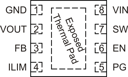
7 Pin Configuration and Functions

DSG Package
8 Pins
Top View
PinAs_lvsaf7.gif

Pin Functions

PIN I/O DESCRIPTION
NAME NO.
EN 6 I Enable input. (1 enabled, 0 disabled). This pin must not be left floating and must be terminated
FB 3 I Voltage feedback pin
GND 1 Ground
ILIM 4 I Adjustable input valley current limit. A resistor to ground programs the current limit. Can be connected to VIN for maximum current.
PG 5 O Output power good (1 good, 0 failure; open drain).If unused, connect to ground or leave floating
SW 7 I Connection for Inductor
VIN 8 I Supply voltage for control stage
VOUT 2 O Boost converter output
Exposed Thermal Pad Must be soldered to achieve appropriate power dissipation and for mechanical reasons. Must be connected to GND.