JAJSH47 March 2019 TPS65653-Q1
PRODUCT PREVIEW Information. Product in design phase of development. Subject to change or discontinuance without notice.
- 1 特長
- 2 アプリケーション
- 3 概要
- 4 改訂履歴
- 5 概要(続き)
- 6 Pin Configuration and Functions
- 7 Specifications
-
8 Detailed Description
- 8.1 Overview
- 8.2 Functional Block Diagram
- 8.3
Feature Description
- 8.3.1 DC/DC Converters
- 8.3.2 Sync Clock Functionality
- 8.3.3 Power-Up
- 8.3.4 Regulator Control
- 8.3.5 Enable and Disable Sequences
- 8.3.6 Device Reset Scenarios
- 8.3.7 Diagnosis and Protection Features
- 8.3.8 Operation of the GPO Signals
- 8.3.9 Digital Signal Filtering
- 8.4 Device Functional Modes
- 8.5 Programming
- 8.6
Register Maps
- 8.6.1
Register Descriptions
- 8.6.1.1 DEV_REV
- 8.6.1.2 OTP_REV
- 8.6.1.3 BUCK0_CTRL_1
- 8.6.1.4 BUCK0_CTRL_2
- 8.6.1.5 BUCK1_CTRL_1
- 8.6.1.6 BUCK1_CTRL_2
- 8.6.1.7 BUCK0_VOUT
- 8.6.1.8 BUCK1_VOUT
- 8.6.1.9 BUCK0_DELAY
- 8.6.1.10 BUCK1_DELAY
- 8.6.1.11 GPO_DELAY
- 8.6.1.12 GPO2_DELAY
- 8.6.1.13 GPO_CTRL
- 8.6.1.14 CONFIG
- 8.6.1.15 PLL_CTRL
- 8.6.1.16 PGOOD_CTRL_1
- 8.6.1.17 PGOOD_CTRL_2
- 8.6.1.18 PG_FAULT
- 8.6.1.19 RESET
- 8.6.1.20 INT_TOP_1
- 8.6.1.21 INT_TOP_2
- 8.6.1.22 INT_BUCK
- 8.6.1.23 TOP_STAT
- 8.6.1.24 BUCK_STAT
- 8.6.1.25 TOP_MASK_1
- 8.6.1.26 TOP_MASK_2
- 8.6.1.27 BUCK_MASK
- 8.6.1.28 SEL_I_LOAD
- 8.6.1.29 I_LOAD_2
- 8.6.1.30 I_LOAD_1
- 8.6.1
Register Descriptions
- 9 Application and Implementation
- 10Power Supply Recommendations
- 11Layout
- 12デバイスおよびドキュメントのサポート
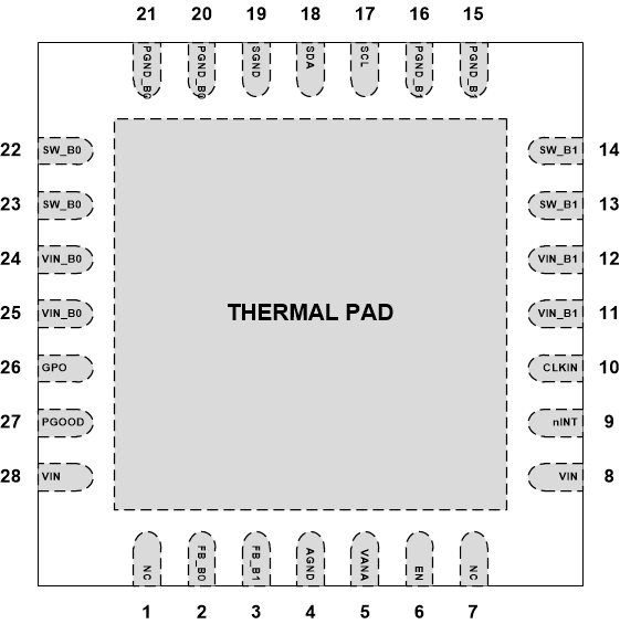
6 Pin Configuration and Functions
RHD Package
28-Pin VQFN With Thermal Pad
Top View

Pin Functions
| PIN | TYPE(1) | DESCRIPTION | |
|---|---|---|---|
| NUMBER | NAME | ||
| 1 | NC | O | Unused. Leave this pin floating. |
| 2 | FB_B0 | A | Output voltage feedback (positive) for Buck 0 |
| 3 | FB_B1 | A | Output voltage feedback (positive) for Buck 1 |
| 4 | AGND | G | Ground |
| 5 | VANA | P/I | Supply voltage for analog and digital blocks. Must be connected to same node with VIN_Bx. |
| 6 | EN | D/I | Programmable enable signal for regulators and GPOs. If the pin is not used, leave the pin floating. |
| 7 | NC | O | Unused. Leave this pin floating. |
| 8 | VIN | I | Unused. Connect this pin to VANA. |
| 9 | nINT | D/O | Open-drain interrupt output. Active LOW. If the pin is not used, connect the pin to ground. |
| 10 | CLKIN | D/I/O | External clock input. Alternative function is general-purpose digital output (GPO2). If the pin is not used, leave the pin floating. |
| 11, 12 | VIN_B1 | P/I | Input for Buck 1. The separate power pins VIN_Bx are not connected together internally - VIN_Bx pins must be connected together in the application and be locally bypassed. |
| 13, 14 | SW_B1 | P/O | Buck 1 switch node. If the Buck 1 is not used, leave the pin floating. |
| 15, 16 | PGND_B1 | P/G | Power ground for Buck 1 |
| 17 | SCL | D/I | Serial interface clock input for I2C access. Connect a pullup resistor. If the I2C interface is not used, connect the pin to Ground. |
| 18 | SDA | D/I/O | Serial interface data input and output for I2C access. Connect a pullup resistor. If the I2C interface is not used, connect the pin to Ground. |
| 19 | SGND | G | Ground |
| 20, 21 | PGND_B0 | P/G | Power ground for Buck 0 |
| 22, 23 | SW_B0 | P/O | Buck 0 switch node. If the Buck 0 is not used, leave the pin floating. |
| 24, 25 | VIN_B0 | P/I | Input for Buck 0. The separate power pins VIN_Bx are not connected together internally - VIN_Bx pins must be connected together in the application and be locally bypassed. |
| 26 | GPO | D/O | General-purpose digital output. If the pin is not used, leave the pin floating. |
| 27 | PGOOD | D/O | Power-good indication signal. If the pin is not used, leave the pin floating. |
| 28 | VIN | I | Unused. Connect this pin to VANA. |
| Thermal Pad | — | — | Connect to PCB ground plane using multiple vias for good thermal performance. |
(1) A: Analog Pin, D: Digital Pin, G: Ground Pin, P: Power Pin, I: Input Pin, O: Output Pin