SLVSCE5B November 2013 – July 2016 DRV3203E-Q1
- 1 Features
- 2 Applications
- 3 Description
- 4 Revision History
- 5 Pin Configuration and Functions
- 6 Specifications
-
7 Detailed Description
- 7.1 Functional Block Diagram
- 7.2 Feature Description
- 7.3
Register Maps
- 7.3.1
Register Descriptions
- 7.3.1.1 CFGUNLK (address 0x01): Configuration Unlock Register
- 7.3.1.2 FLTCFG (address 0x02): Fault Detection Configuration Register
- 7.3.1.3 FLTEN0 (address 0x04): FAULT Pin Enable Register 0
- 7.3.1.4 FLTEN1 (address 0x05): FAULT Pin Enable Register 1
- 7.3.1.5 SDNEN0 (address 0x06): Pre-Driver Shutdown Enable Register 0
- 7.3.1.6 SDNEN1 (address 0x07): Pre-Driver Shutdown Enable Register 1
- 7.3.1.7 FLTFLG0 (address 0x08): Fault Flag Register 0
- 7.3.1.8 FLGFLT1 (address 0x09): Fault Flag Register 1
- 7.3.1.9 CSCFG (address 0x0A): Current Sense Configuration Register
- 7.3.1.10 PDCFG (address 0x0B): Pre-Driver Configuration Register
- 7.3.1.11 DIAG (address 0x0C): Diagnosis Register
- 7.3.1.12 SPARE (address 0x0D): Spare Register
- 7.3.1
Register Descriptions
- 8 Application and Implementation
- 9 Device and Documentation Support
- 10Mechanical, Packaging, and Orderable Information
1 Features
- Qualified for Automotive Applications
- AEC-Q100 Qualified with the Following Results:
- Device Temperature Grade 0: –40℃ to 150℃ Ambient Operating Temperature Range
- Device HBM ESD Classification Level H2
- Device CDM ESD Classification Level C2
- 3-Phase Pre-Drivers for N-Channel MOS Field-Effect Transistors (MOSFETs)
- Pulse-Width Modulation (PWM) Frequency up to 20 kHz
- Fault Diagnostics
- Charge Pump
- Phase Comparators
- Microcontroller (MCU) Reset Generator
- Serial Port I/F (SPI)
- Motor-Current Sense
- 3.3-V Regulator
- Low-Current Sleep Mode
- Operation VB Range From 5.3 to 26.5 V
- 48-Pin PHP
2 Applications
- Automotive Motor-Control Applications
- Oil Pump
- Fuel Pump
- Water Pump
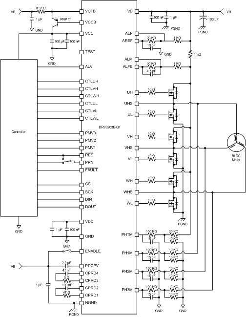
Typical Application Schematic

3 Description
The DRV3203E-Q1 device is a field-effect transistor (FET) pre-driver designed for three-phase motor control for applications such as an oil pump or a water pump. The device has three high-side pre-FET drivers and three low-side drivers which are under the control of an external MCU. A charge pump supplies the power for the high side, and there is no requirement for a bootstrap capacitor. For commutation, this integrated circuit (IC) sends a conditional motor signal and output to the MCU. Diagnostics provide undervoltage, overvoltage, overcurrent, overtemperature and power-bridge faults. One can measure the motor current using an integrated current-sense amplifier and comparator in a battery common-mode range, which allows the use of the motor current in a high-side current-sense application. External resistors set the gain. One can configure the pre-drivers and other internal settings through the SPI.
Device Information(1)
| PART NUMBER | PACKAGE | BODY SIZE (NOM) |
|---|---|---|
| DRV3203E-Q1 | HTQFP (48) | 7.00 mm × 7.00 mm |
- For all available packages, see the orderable addendum at the end of the datasheet.
4 Revision History
Changes from A Revision (January 2014) to B Revision
- Added Pin Configuration and Functions section, ESD Ratings table, Feature Description section, Application and Implementation section, Device and Documentation Support section, and Mechanical, Packaging, and Orderable Information section Go
Changes from * Revision (November 2013) to A Revision
- Changed symbol for the Data delay time, SCK to DOUT parameter in the SPI ELECTRICAL CHARACTERISTICS table from tv to td Go
- Changed the delay time, SCK to DOUT image reference from Figure 23 to Figure 2 in the SPI ELECTRICAL CHARACTERISTICS tableGo
- Changed the max value for the RONH_HP parameter from 310 to 300 in the Pre-Driver Electrical Characteristics tableGo
- Deleted the 1 from the symbols for the time parameters (ton_h, toff_h , th-on, and th-off) for the high-side pre-driver in the Pre-Driver Electrical Characteristics tableGo
- Changed the max for the VOL_L parameter from 55 to 60 in the Pre-Driver Electrical Characteristics tableGo
- Changed the max for the RONL_L parameter from 5 to 6 in the Pre-Driver Electrical Characteristics tableGo
- Changed the symbol for the turnoff time parameter for the low-side pre-driver from toff_h to toff_l in the Pre-Driver Electrical Characteristics tableGo
- Changed conditions of Tset_TR2, Tset_TF2 and OVADth in the Motor Current-Sense Electrical Characteristics tableGo
- Changed the value for the VCCUVHYS parameters in the VCC and VDD Electrical Characteristics table from 50, 100, and 200 to 33, 66, and132Go
- Added ADTH to the bit 6:4 description in the FLTCFG register table Go
- Changed the description for writing a 0 to bit 2 in the FLTCFB register table from 2.3 to 2.2 VGo
- Changed the dead time description for bit 1:0 in the PDCFG register table from 2, 1.5, 1, and 0.5 to 2.1, 1.6, 1.1, and 0.6 (respectively). Also changed the actual deadtime from ±0.2 to ±0.1Go