JAJU299A June 2017 – January 2023
- 概要
- リソース
- 特長
- アプリケーション
- 5
- 1System Description
-
2System Overview
- 2.1 Block Diagram
- 2.2 Highlighted Products
- 2.3 Design Considerations
- 3Getting Started Hardware
- 4Testing and Results
- 5Design Files
- 6Related Documentation
- 7Trademarks
- 8Revision History
2.3.3.2 Stability Limits and Output Capacitor Selection
The "recommended" curve in Figure 4-1 shows the recommended maximum output current based on stability. The TIDA-01457 design must be operated at load currents below this line. In most applications, which have ambient temperatures above 25°C, the thermal limit lines move down below the recommended line (as explained in Section 2.3.3.1), which further limits the maximum output current.
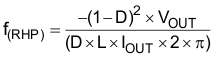
The inverting buck-boost topology contains a right-half plane zero, which significantly and negatively impacts the control loop response by adding an increase in gain along with a decrease in phase at a high frequency. This right-half plane zero can cause instability. Equation 6 estimates the frequency of the right-half plane zero.
The TIDA-01457 design uses four 22-µF output capacitors, which have an effective capacitance of about 36 µF at the –5-V output voltage. This amount of capacitance pushes the crossover frequency of the control loop down to frequencies low enough so that the right-half plane zero is sufficiently higher in frequency for stability. While one of these output capacitors requires placement near the TPS82130 device, the others can be placed at the point of load and serve as their input decoupling capacitor. When three of the output capacitors are placed at the point of load, the solution size is below 50 mm2. If these three capacitors are included, the solution size of all components shown within the Active Circuitry box on the front page becomes around 75 mm2.
More output capacitance improves stability by increasing the separation between the right-half plane zero and crossover. The right-half plane zero frequency occurs at lower frequencies with lower input voltages, which have a higher duty cycle. Load transient testing is the best test for stability, as described in the Simplifying Stability Checks application report. Because the VOS pin of the TPS82130 is connected on the device, it is impossible to break the entire control loop and measure a bode plot.