JAJU299A June 2017 – January 2023
- 概要
- リソース
- 特長
- アプリケーション
- 5
- 1System Description
-
2System Overview
- 2.1 Block Diagram
- 2.2 Highlighted Products
- 2.3 Design Considerations
- 3Getting Started Hardware
- 4Testing and Results
- 5Design Files
- 6Related Documentation
- 7Trademarks
- 8Revision History
4 Testing and Results
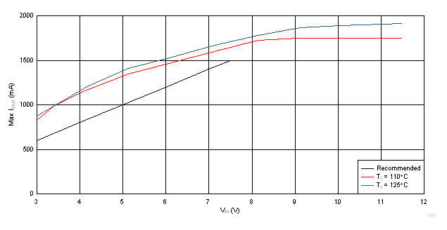 Figure 4-1 Maximum Output Current
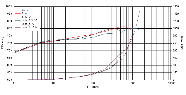 Figure 4-2 Efficiency Over Load
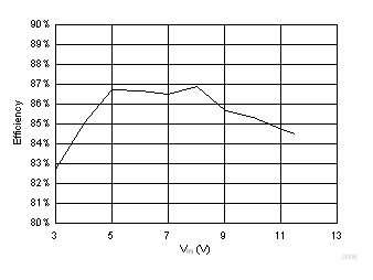 Figure 4-3 Efficiency Over VIN (600-mA Load)
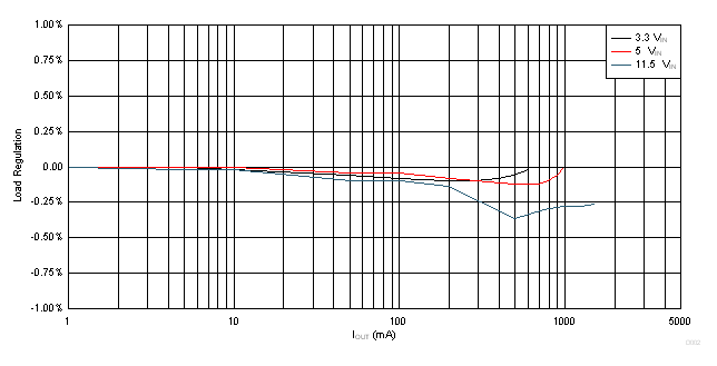 Figure 4-4 Load Regulation
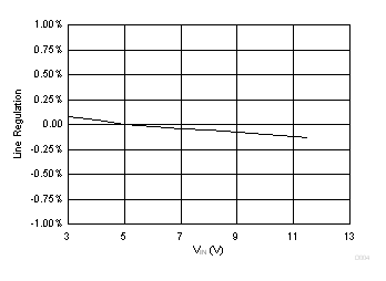 Figure 4-5 Line Regulation (600-mA Load)
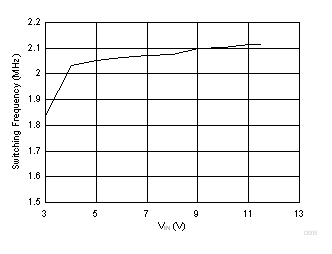 Figure 4-6 Switching Frequency Over VIN (600-mA Load)
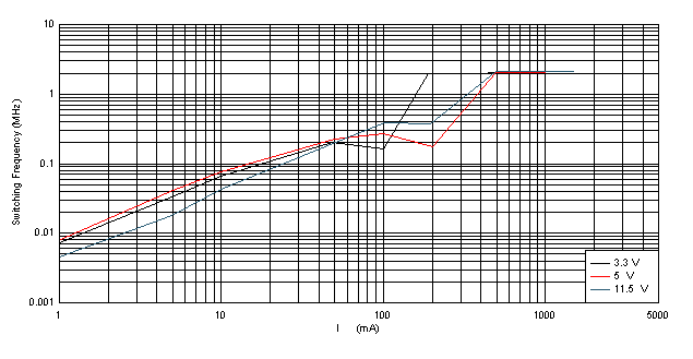 Figure 4-7 Switching Frequency Over Load
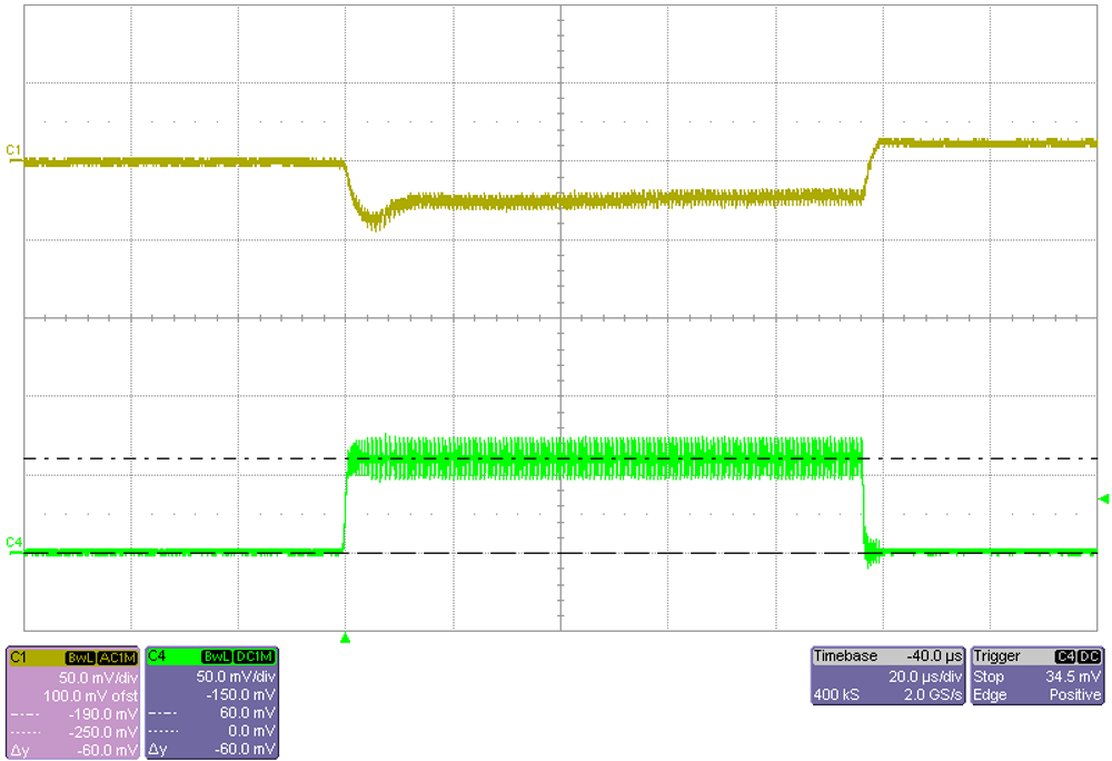 Figure 4-8 Transient Response (3.3 VIN, 0- to 600-mA Load Step)
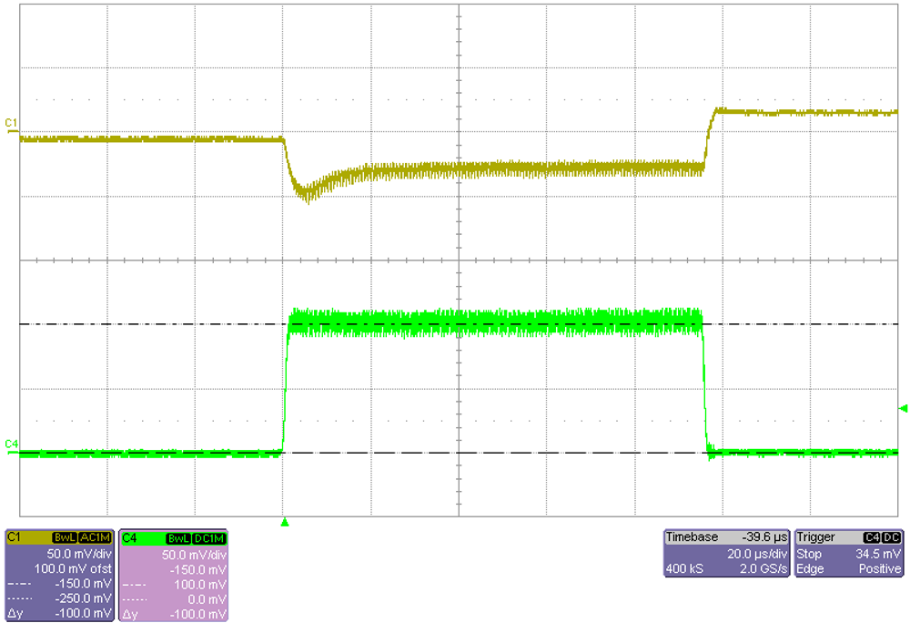 Figure 4-9 Transient Response (5 VIN, 0- to 1-A Load Step)
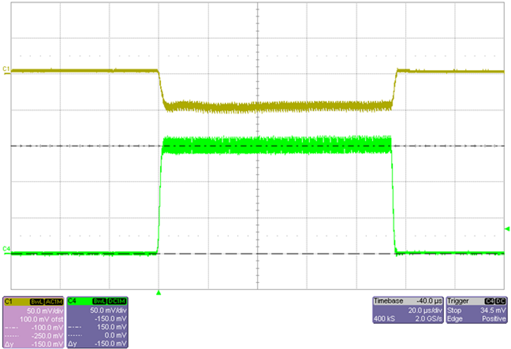 Figure 4-10 Transient Response (7.5 VIN, 0- to 1.5-A Load Step)
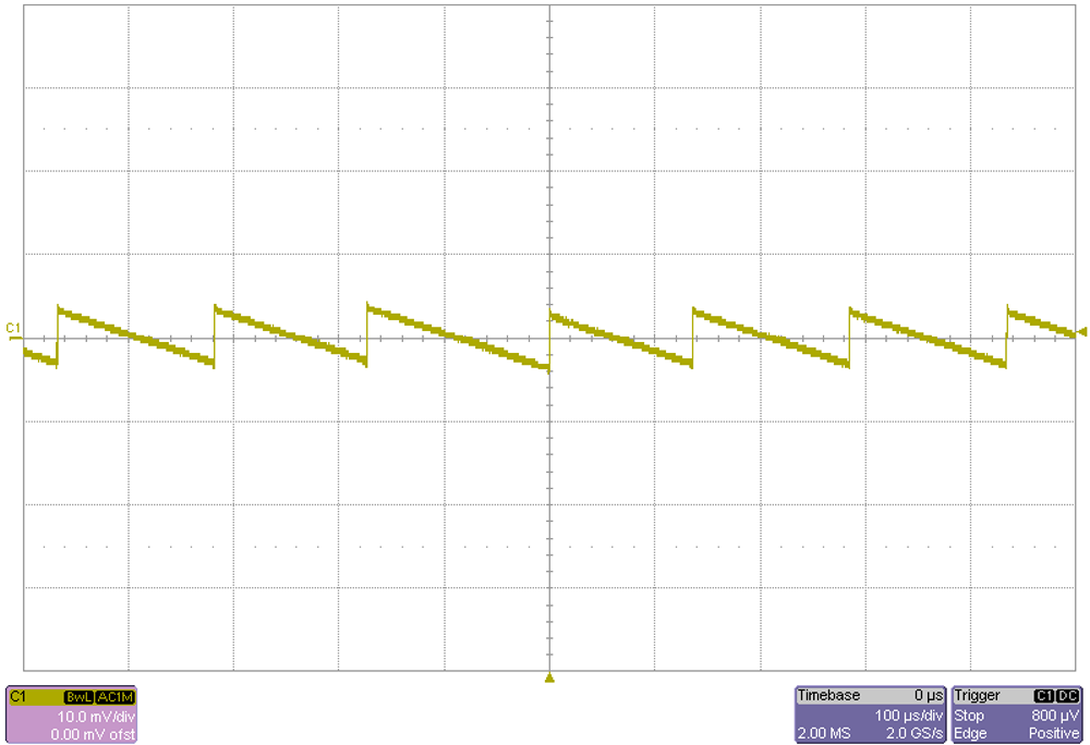 Figure 4-11 Output Voltage Ripple (3.3 VIN, 1-mA Load)
 Figure 4-12 Output Voltage Ripple (3.3 VIN, 600-mA Load)
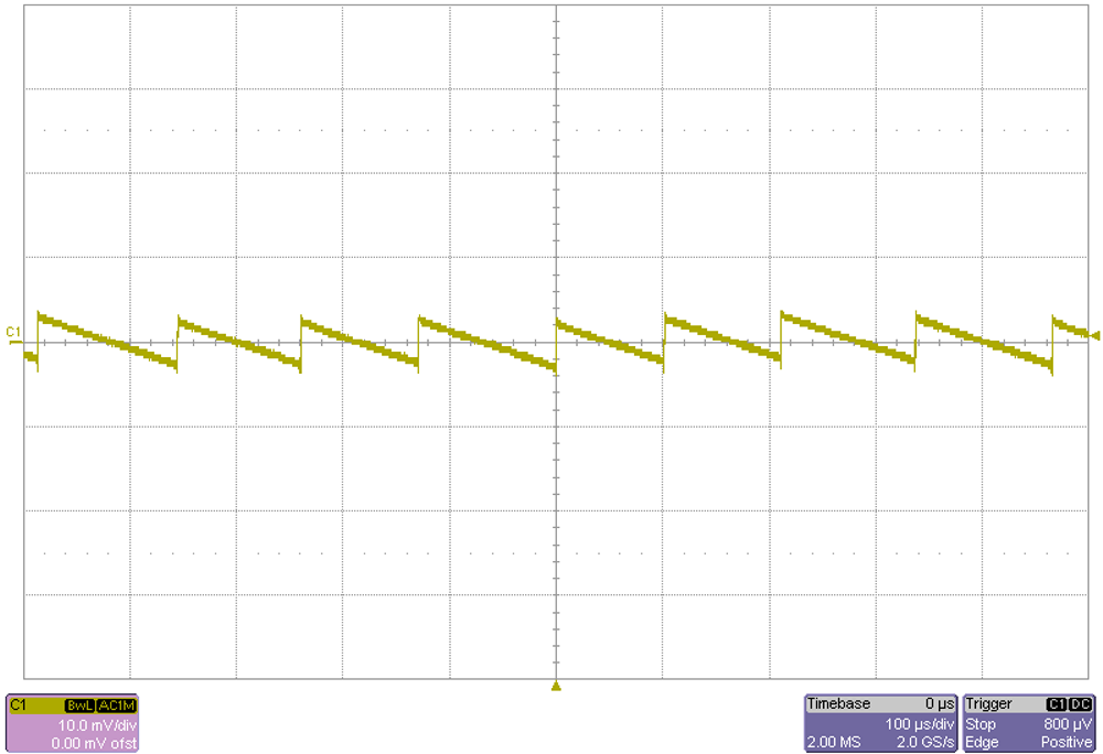 Figure 4-13 Output Voltage Ripple (5 VIN, 1-mA Load)
 Figure 4-14 Output Voltage Ripple (5 VIN, 1-A Load)
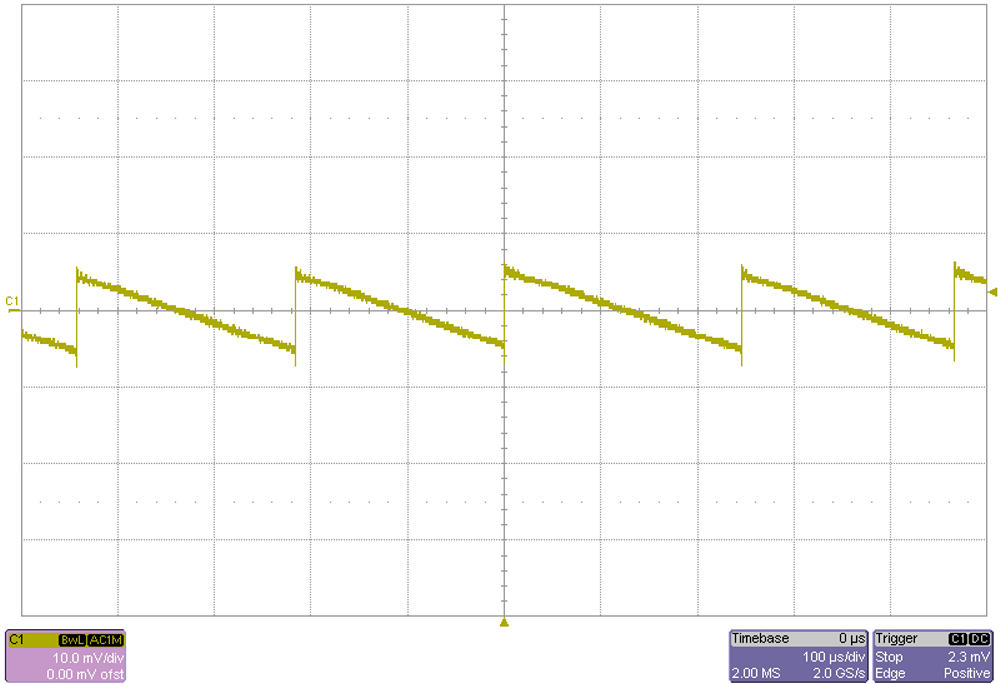 Figure 4-15 Output Voltage Ripple (11.5 VIN, 1-mA Load)
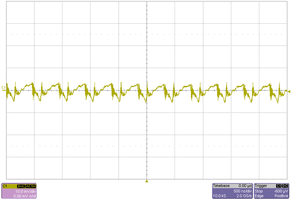 Figure 4-16 Output Voltage Ripple (11.5 VIN, 1.5-A Load)
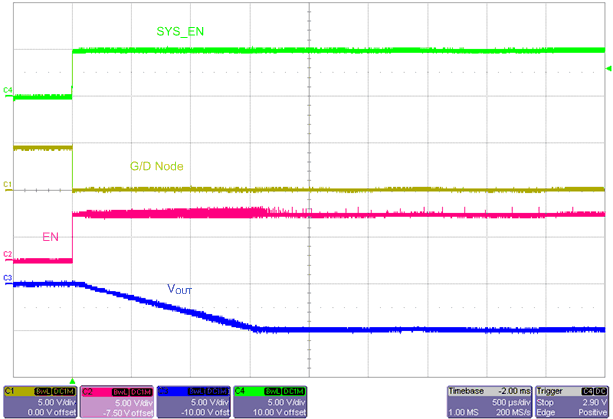 Figure 4-17 Start-up on EN (5 VIN, No Load)
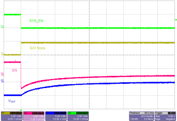 Figure 4-18 Shutdown on EN (5 VIN, No Load)
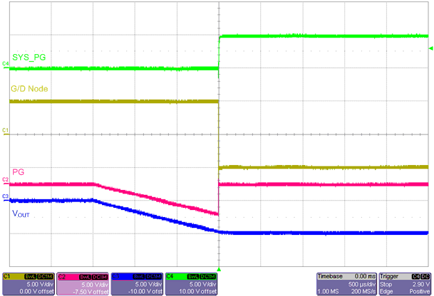 Figure 4-19 PG on Start-up (5 VIN, No Load)
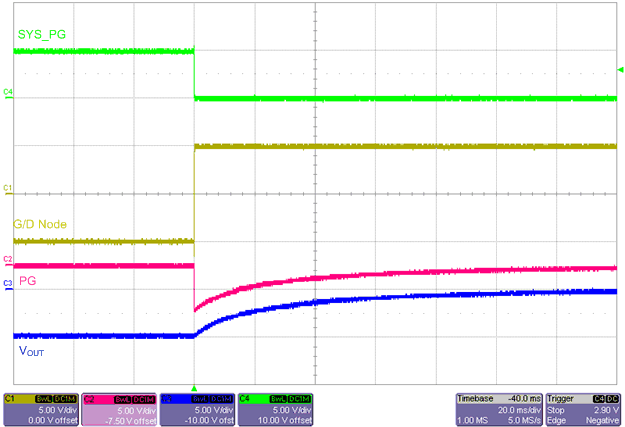 Figure 4-20 PG on Shutdown (5 VIN, No Load)