JAJU299A June 2017 – January 2023
- 概要
- リソース
- 特長
- アプリケーション
- 5
- 1System Description
-
2System Overview
- 2.1 Block Diagram
- 2.2 Highlighted Products
- 2.3 Design Considerations
- 3Getting Started Hardware
- 4Testing and Results
- 5Design Files
- 6Related Documentation
- 7Trademarks
- 8Revision History
2.3.1 Inverting Buck-Boost Topology Concept
The inverting buck-boost topology is very similar to the buck topology. In the buck configuration that Figure 2-2 shows, the positive connection (VOUT) is connected to the VOUT pin of the power module and the return connection is connected to the ground (GND) of the power module. However, in the inverting buck-boost configuration that Figure 2-3 shows, the power module ground is used as the negative output voltage pin (labeled as –VOUT). The terminal formerly known as the positive output in the buck configuration is used as the ground. This inverting topology allows the output voltage to be inverted and always lower than the ground.
 Figure 2-2 TPS82130 Buck Topology
 Figure 2-3 TPS82130 Inverting Buck-Boost Topology
The circuit operation is different in the inverting buck-boost topology than in the buck topology. Figure 2-4 (a) shows that the output voltage terminals are reversed, though the components are wired the same as a buck converter. As Figure 2-4 (b) shows, during the ON-time of the control MOSFET, the inductor is charged with current while the output capacitor supplies the load current. The inductor does not provide current to the load during this time. During the OFF-time of the control MOSFET and the ON-time of the synchronous MOSFET (see Figure 2-4 (c)), the inductor provides current to the load and the output capacitor. These changes affect many parameters, which the following subsections describe in further detail.
 Figure 2-4 Inverting
Buck-Boost Configuration
Figure 2-4 Inverting
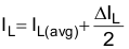
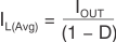
Buck-Boost ConfigurationThe average inductor current is affected in this topology. In the buck configuration, the average inductor current is equal to the average output current because the inductor always supplies current to the load during both the ON- and OFF-times of the control MOSFET. However, in the inverting buck-boost configuration, only the output capacitor supplies the load with current, while the load is completely disconnected from the inductor during the ON-time of the control MOSFET. During the OFF-time, the inductor connects to both the output capacitor and the load (see Figure 2-4). Because the OFF-time is 1 – D of the switching period, the average inductor current in Equation 1 is calculated as:
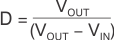
The duty cycle for the typical buck converter is simply VOUT / VIN, but the calculation of the duty cycle in Equation 2 for an inverting buck-boost converter becomes:
Equation 3 provides the peak-to-peak inductor ripple current:

where:
- ΔIL (A): Peak-to-peak inductor ripple current
- D: Duty cycle
- fS (MHz): Switching frequency
- L (µH): Inductor value of typically 1 µH
- VIN (V): Input voltage with respect to ground, not with respect to the device ground or VOUT
Equation 4 calculates the maximum inductor current: