JAJU633 October 2018
- 概要
- リソース
- 特長
- アプリケーション
- デザイン・イメージ
- 1System Description
-
2System Overview
- 2.1 Block Diagram
- 2.2 Highlighted Products
- 2.3 LM74700
- 2.4
System Design Theory
- 2.4.1
Design Procedure
- 2.4.1.1 Operating Parameters, Duty Cycle
- 2.4.1.2 Setting the Switching Frequency
- 2.4.1.3 Inductor Value Calculation
- 2.4.1.4 Peak Inductor Current
- 2.4.1.5 Calculating RIS (R9)
- 2.4.1.6 Minimum Output Capacitance
- 2.4.1.7 Setting the LED Current
- 2.4.1.8 Soft-Start Capacitor
- 2.4.1.9 Overvoltage Protection (OVP)
- 2.4.1.10 Main N-Channel MOSFET Selection
- 2.4.1.11 Rectifier Diode Selection
- 2.4.1.12 Thermal Protection
- 2.4.2 Designing for Low EMI
- 2.4.1
Design Procedure
- 3Hardware, Software, Testing Requirements, and Test Results
- 4Design Files
- 5Related Documentation
3.2.2.1 Nominal Operation Waveforms
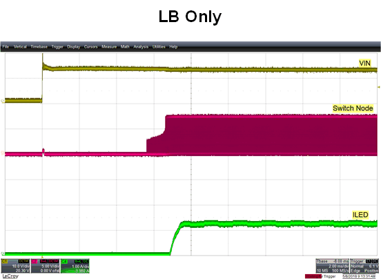 Figure 9. Low Beam Mode Startup—CH1: VIN, CH2: Switch Node
(Q3 Drain) Voltage, and CH4: LED Current
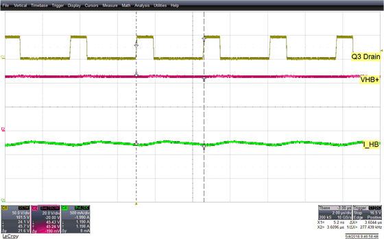 Figure 11. Normal Operation Fswitch at 275 KHz—
CH1: Switch Node (Q3 Drain), CH2: VLED in High Beam and Low Beam Mode,
and CH4: LED Current for Ouput power of 55 W
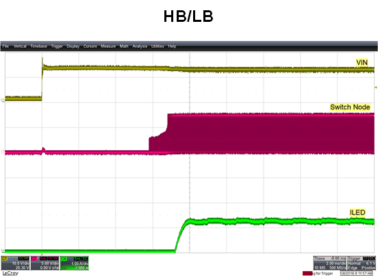 Figure 10. High Beam/Low Beam Mode Steady State Switching—CH2: Switch Node (Q3 Drain) Voltage
and CH4: LED Current for Ouput power of 55 W
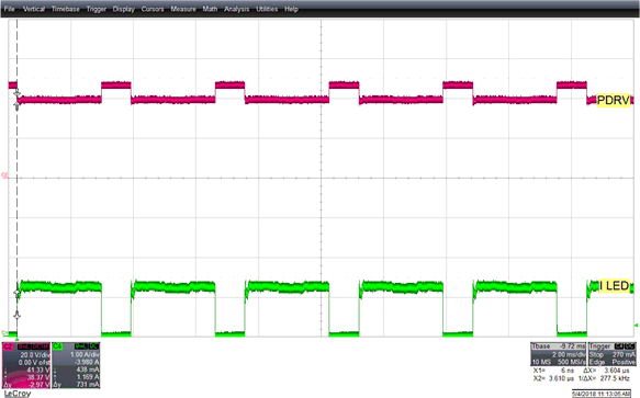 Figure 12. 240 Hz, 33% Duty Cycle PWM Dimming Feature with R18 (100 KΩ)—
CH1: PDRV, and CH4: LED Current
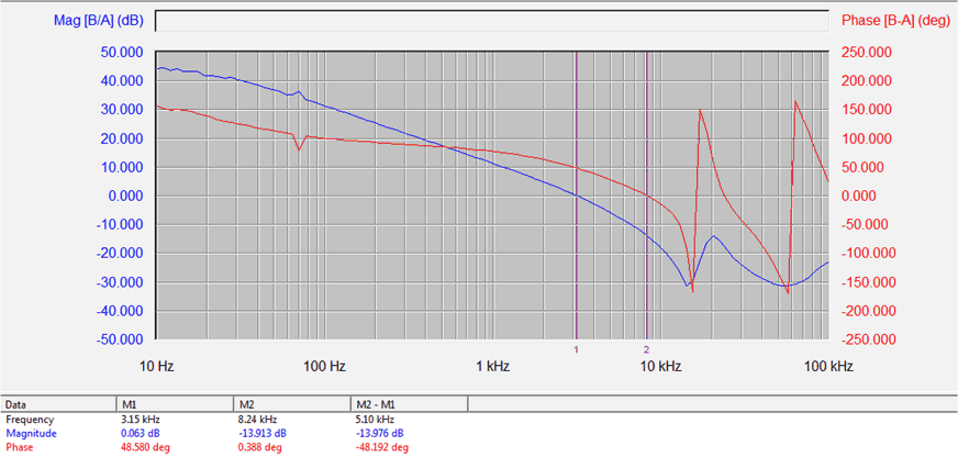 Figure 13. Gain Phase Margin for LB only in Buck Boost Mode (7 LEDs at 27.5 W)
Cross Over: 3.15 kHz Phase Margin: 48.6 Degree Gain Margin: 13.9 dB
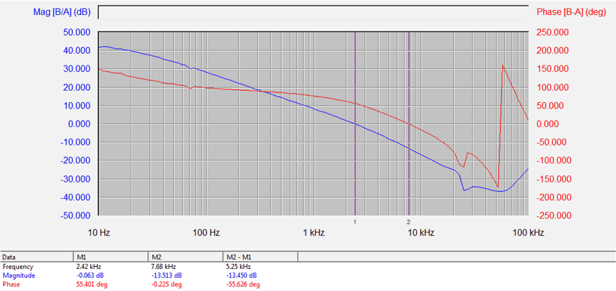 Figure 14. Gain Phase Margin for HB/LB Boost Mode 55 W (Low Beam: 7 LEDs HB: 7 LEDs)
Cross Over: 2.42 kHz Phase Margin: 55.4 Degree Gain Margin: 13.5 dB
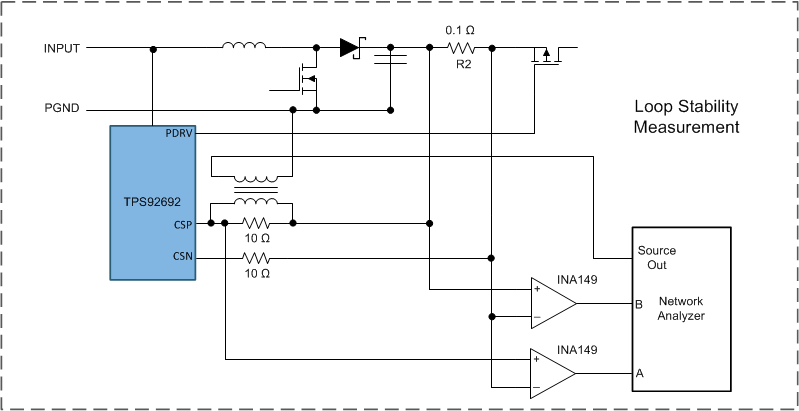
Section 3.2.2.1.1 shows the network analyzer circuit that measures loop stability. In addition, a pair of differential amplifier (INA149) is used to remove high common mode DC voltage from the signal feeding back to the Network Analyzer. An isolation amplifier is used to generate the injection signal. The requirement of INA149 differential amplifiers is to remove high common mode voltage which exceed the input range of the Network Analyzer for gain and phase margin measurements.
3.2.2.1.1 Loop Stability Measurements Block Diagram
