SBAU362 March 2021 ADS1015 , ADS1115
3.3 Analog Input Connections
The ADS1x15 device is designed for easy interface to an external sensor that is differential or single-ended using either a header (J6) or a screw terminal block (J5). Connector J6 provides an easy interface connection for differential input pairs with each pair separated by analog ground. Table 3-2 lists the channel input connections for J5 and Table 3-3 shows the input connections for J6. Both connectors are clearly labeled on the PCB silkscreen for easy input connection identification.
| J5 Terminal Block Inputs | Description |
|---|---|
| J5:1 | Analog input for AIN0 of the ADC |
| J5:2 | Analog input for AIN1 of the ADC |
| J5:3 | Analog input for AIN2 of the ADC |
| J5:4 | Analog input for AIN3 of the ADC |
| J5:5 | Analog ground |
| J6 Terminal Block Inputs | Description |
|---|---|
| J6:1 | Analog input for AIN0 of the ADC |
| J6:2 | Analog input for AIN1 of the ADC |
| J6:3 and J6:4 | Analog ground |
| J6:5 | Analog input for AIN2 of the ADC |
| J6:6 | Analog input for AIN3 of the ADC |
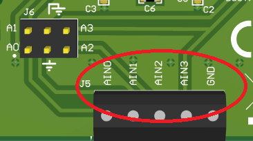
Connector J5 is a screw terminal block for attaching an external sensor with bare wire connections. The terminal block includes all four inputs and a connection point for analog ground. Figure 3-2 shows the input layout.
 Figure 3-2 Analog Input Terminal Block (J5)
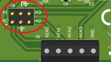
Connector J6 is a 100-mil spaced dual-row header. Jumper wire or clip leads can be used for connections. The header includes all four inputs and two analog ground connections. Figure 3-3 shows the input layout.
 Figure 3-3 Analog Input Header (J6)
Each analog input includes a single-order, low-pass filter. The single-ended input filter cutoff frequency is 67.9 kHz. Up to four separate single-ended measurements are possible.
Instead of single-ended measurements, up to two differential input pair combinations are possible. The filter design for the differential input pair filtering has a cutoff frequency of 3.4 kHz. The filter is populated on the ADS1x15EVM for input pair combinations of AIN0 and AIN1 or AIN2 and AIN3. The input combination of AIN1 and AIN2 is possible by adding a 47-nF capacitor at C6 (see location in Figure 6-5).
The configuration options for the ADS1x15 allow for a potential full-scale range (FSR) greater than the supply. This increased range is useful when an input voltage slightly exceeds the next lower FSR. However, the input voltage should not exceed the range of the VDD supply selected at JP1. The absolute input voltage is bounded by VDD + 0.3 V and GND – 0.3 V. Damage to the ADS1x15 may occur if the absolute input range is exceeded.