SCEA047B November 2013 – November 2022 SN74LV1T00 , SN74LV1T02 , SN74LV1T04 , SN74LV1T08 , SN74LV1T32 , SN74LV1T86
5 Example Application 2: PGOOD Circuit
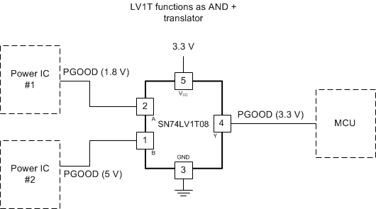
In this example, the engineer wants to send a signal to the MCU when both power ICs have been ramped to their appropriate output levels. Normally, this application would require an AND gate, combined with appropriate translators for each level. The SN74LV1T08 2-input AND gate can accept input voltages different than its supply (VCC), even when the A and B inputs are at different voltage levels. The LVxT device allows the engineer to use a single device in the place of the AND gate and translators, which could have previously required up to three separate devices.
 Figure 5-1 Power good schematic with
SN74LV1T08 operating with mixed input voltages