SCEA143 December 2023 SN74AVC8T245 , SN74AVC8T245-Q1 , SN74AXC8T245 , SN74AXC8T245-Q1 , TXV0106 , TXV0106-Q1 , TXV0108 , TXV0108-Q1
3.4 Leveraging TXV for High-Bandwidth Applications
| Parameter - 560Mbps | TXV (V) | Competitor (V) | Valid Levels (V) {0.7*Vcco and 0.3*Vcco} |
|---|---|---|---|
| VOH | 2.6 | 1.8 | > 2.31 |
| VOL | 0.032 | 1.3 | < 0.99 |
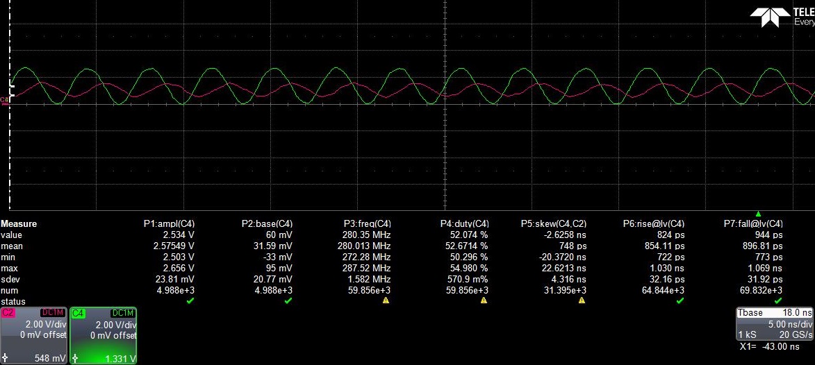
- Figure 3-9 shows typical bench data for TXV (1.8 V red inputs, 3.3 V green outputs) running at 560Mbps (280 MHz) with stable VOH (as high as 2.6 V) and stable VOL (as low as 32 mV).
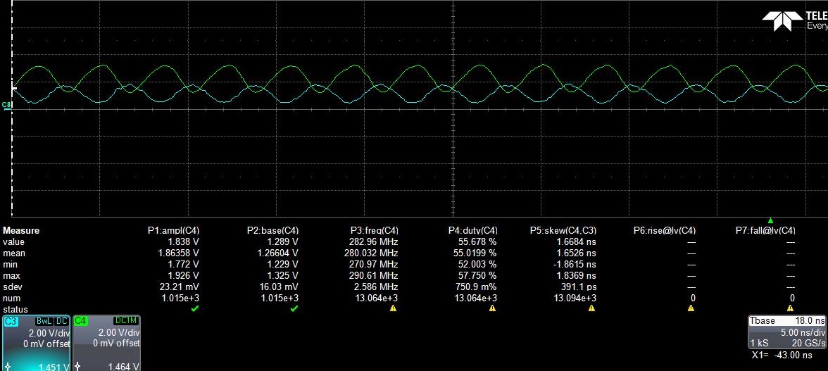
- Figure 3-10 shows how competitor can fail (1.8 V blue inputs, 3.3 V green outputs) with unstable VOH (as low as 1.9 V) and unstable VOL (as high as 1.3 V) for invalid logic switching levels.
 Figure 3-9 TXV Waveform (15 pF 1.8 V to 3.3 V Up Translation at 280 MHz, 25°C)
 Figure 3-10 Competitor Waveform (15 pF 1.8 V to 3.3 V Up Translation at 280 MHz, 25°C)
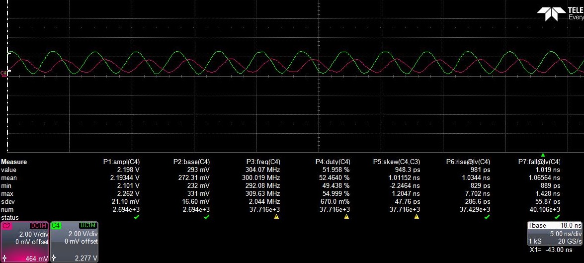
For interfaces higher than 560Mbps (280 MHz), Figure 3-11 shows typical bench data with TXV (1.8 V red inputs, 3.6 V green outputs) running at 600Mbps (300 MHz) with VOH / VOL levels at 2.2 V and 0.3 V respectively, measuring low propagation delay (as fast as 1 ns), with 15 pF load.
 Figure 3-11 TXV Outputs (15 pF 1.8 V to 3.6 V Up Translation at 300 MHz, 25°C)
For typical applications such as 3.3 V, TI’s TXV0108 measured faster data throughput with stable outputs while competitor can fail with unstable outputs as shown in Table 3-5, with damages prevalent. Switching around 1/2 of the output's Vcc can lead to increased current draw with the likelihood of damaging the device if above the absolute maximum ratings. Refer to Implications of Slow or Floating CMOS Inputs, for additional information.