SLOA277B january 2019 – july 2023 LM124 , LM124-N , LM124A , LM158 , LM158-N , LM158A , LM224 , LM224-N , LM224A , LM258 , LM258-N , LM258A , LM2902 , LM2902-N , LM2902-Q1 , LM2902K , LM2902KAV , LM2904 , LM2904-N , LM2904-Q1 , LM2904B , LM2904B-Q1 , LM2904BA , LM321 , LM324 , LM324-N , LM324A , LM358 , LM358-N , LM358A , LM358B , LM358BA , TS321 , TS321-Q1
2.3 Input Impedance
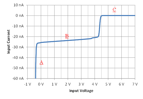
The input stage uses a Darlington PNP configuration with dedicated internal current sources on all of the transistor emitters. Therefore the input appears as a current source to the application. This current is the input PNP transistor's base current whose value is specified in the data sheet as IIB. This effective input current source has a high impedance of approximately 1 GΩ and a wide voltage range compliance from 0 V to one diode drop below VCC, including cases where a large differential input voltage is present (see Figure 2-3 region B). When the input voltage is greater than one diode voltage drop below VCC or is greater than VCC, the input becomes high impedance and no current flows other than a reverse diode leakage current (see Figure 2-3 region C). Matching the input resistance can reduce the input offset voltage from IIB. This can be done by placing matching resistors on the inputs. Note that the consequential increase in resistor thermal noise may be unacceptable.
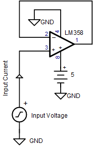
The input current profile for a unity gain buffer powered by a 5-V supply, shown in Figure 2-2, can be seen in Figure 2-3. Applying a negative input voltage will forward bias a diode formed from the input PNP transistor's base to the die’s grounded substrate on the input pin. The result will be high current flow as indicated by the vertical slope near –0.5 V (region A). An input between 0 V and 3.5 V (region B) has a fixed current (IIB) with an impedance of approximately 1 GΩ. Region C spans from 4.5 V to 7 V and beyond, continuing up to a maximum of VCC where there is no input current flow.
 Figure 2-2 Unity Gain Buffer Test
Configuration
 Figure 2-3 Input Current vs Input
Voltage
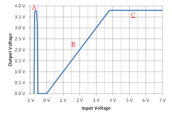
 Figure 2-4 Output Voltage vs Input
Voltage